PCB circuit board plasma cutting machine etching technology
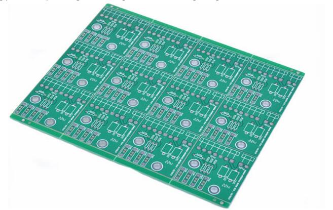
The production of high-density multilayer boards by circuit board manufacturers requires plasma cutting machine eroding and plasma cleaning machine. The general production process flow chart is: PCB core board processing - coating to form coating agent - pressing and coating resin copper foil -Transfer the pattern into a plasma etching window-plasma cutting and etching the via hole-chemical electroplating copper processing-pattern transfer to form an electrical interconnection conductive pattern-surface treatment.
1. Technical characteristics of plasma cutting
The plasma temperature is high, it can provide a high enthalpy working medium, produce materials that cannot be obtained by conventional methods, and have the advantages of controllable atmosphere, relatively simple equipment, and significantly shorten the process flow, so the plasma animal sculpture technology has great develop. In 1879, W. Crooks pointed out that the ionized gas in the discharge tube is the fourth state of matter different from gas, liquid, and solid. In 1928, I. Langmuir named it plasma. The most common plasmas are arc, neon and fluorescent gas, lightning, aurora, etc. With the development of science and technology, people have been able to artificially generate plasma in a variety of ways, thus forming a widely used plasma technology. Generally speaking, plasma with a temperature of about 108K is called high-temperature plasma, which is currently only used in controlled thermonuclear fusion experiments; plasma with industrial application value has a temperature between 2*103~5*104K and can be sustained Low-temperature plasma for a few minutes or even dozens of hours is mainly obtained by gas discharge and combustion methods. Gas discharge is divided into arc discharge, high-frequency induction discharge and low-pressure discharge. The plasma produced by the former two is called thermal plasma, which is mainly used as a high-temperature heat source; the plasma produced by the latter is called cold plasma, which has special physical properties that can be used in industry. However, in the treatment of organic waste gas, due to high voltage discharge, it is necessary to prevent explosion accidents that are easy to ignite.

2. The process of plasma cutting and etching process for PCB board processing is as follows:
This is a resin or adhesive coated (screen printing or spraying or curtain coating) on the "PCB core board" with conductive patterns or on the inner conductive pattern. In addition to having good performance In addition to combining with resin-coated copper foil, it should also have a surface that fills the gaps between the conductive patterns on the circuit board and covers the conductive patterns, so it must have a good conformability. In addition, after coating, it will permanently exist as the dielectric layer of the PCB circuit board. Therefore, its glass transition temperature and dielectric constant should meet the electrical performance, mechanical and physical characteristics of the PCB circuit board. After coating the coating agent on the circuit board, it is in a semi-cured state after drying.
Note: If the circuit board uses a thicker resin-coated copper foil, that is, the semi-cured state of the resin-coated layer is thicker and the vacuum laminator is used for lamination, the step of coating the coating agent is not required.
Resin-coated copper foil refers to coating a layer of resin (such as epoxy, BT, polyphenol imine, etc.) on the surface of the processed (roughened or oxidized) circuit board copper foil with a thickness of about 50um to 80um. After drying (in a semi-cured state) into a roll. On the prepared "PCB core board", use a vacuum laminator or a laminator or a roller to press the resin-coated copper foil. And under controlled temperature (depending on resin type and pressing method), such as epoxy resin and vacuum press, it can be laminated at 170 degree Celsius and 5-20kg/cm pressure, or it can be carried out at lower temperature, And then carry out post-curing treatment. Vacuum lamination helps the resin to fill the gaps and side seams between the conductor patterns on the surface of the "PCB core board", thus eliminating the need for the coating process, shortening the cycle, and saving the production cost of circuit analysis. It must be pointed out that the Tg, dielectric constant and thickness of these "coated resins" that exist as the dielectric layer of the PCB circuit board should meet the requirements of the electrical and physical characteristics of the PCB circuit board. Among them, Tg should be greater than 150 degrees Celsius and the dielectric constant should be less than or equal to 4.0 in most cases.
This step is the same as the conventional PCB circuit board graphics transfer manufacturing process. A laminate formed by pasting and curing resin-coated copper foil, the surface of which is exposed by wiping or roughening the surface of the copper foil, drying and pressing a photosensitive resist dry film, followed by exposure and development The copper foil to be etched away. Then perform acid etching (acid copper chloride etching solution or sulfuric acid plus hydrogen peroxide etching solution) to form a micro via pattern that can be etched by plasma (that is, the resin-coated part is exposed), and then the dry film resist on the circuit board is removed .
3. Application of plasma machining
The high-temperature and high-speed jet generated by the plasma spray gun can be used for mechanical processing such as welding, surfacing, spraying, cutting, heating and cutting. Plasma arc welding is much faster than argon tungsten arc welding. The micro plasma arc welding that came out in 1965, the torch size is only 2 to 3 mm, which can be used to process very small workpieces. Plasma arc surfacing can be used to surfacing wear-resistant, corrosion-resistant, and high-temperature-resistant alloys on components, and is used to process various special valves, drills, tools, molds, and crankshafts. Using the high temperature and strong spray force of the arc plasma, metal or non-metal can be sprayed on the surface of the workpiece to improve the wear resistance, corrosion resistance, high temperature oxidation resistance, and shock resistance of the workpiece. Plasma cutting is to use arc plasma to quickly heat the cut metal to a molten state, and at the same time use a high-speed airflow to blow off the molten metal to form a narrow incision. Plasma heating cutting is to properly set a plasma arc in front of the tool to heat the metal before cutting, change the mechanical properties of the processed material, and make it easy to cut. This method improves work efficiency by 5-20 times compared with conventional cutting methods.
The above is the basic production process of the plasma etching process of PCB circuit board manufacturers.