As we mentioned before, a single-sided PCB is called a single-sided (Single-sided). Because single-sided boards have many strict restrictions on the design of the circuit (because there is only one side, the wiring can not be crossed * and must be a separate path), so only early circuits use this type of board.
Double panel
This kind of circuit board has wiring on both sides. However, to use wires on both sides, there must be a proper circuit connection between the two sides. This kind of "bridge" between circuits is called a via. A via is a small hole filled or coated with metal on the PCB, which can be connected with the wires on both sides. Because the area of the double panel is twice as large as that of the single panel, and because the wiring can be interleaved (it can be wound to the other side), it is more suitable for use in circuits that are more complicated than the single panel.
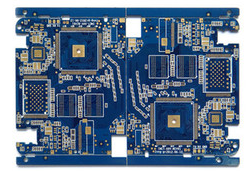
Multilayer board
[Multilayer board] For more complex application requirements, the circuit can be arranged in a multi-layer structure and pressed together, and through-hole circuits are arranged between the layers to connect the circuits of each layer.
Inner line

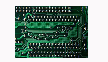
Four-layer circuit board
The copper foil substrate is first cut into a size suitable for processing and production. Before the substrate is laminated, it is usually necessary to roughen the copper foil on the surface of the board by brushing, microetching, etc., and then attach the dry film photoresist to it with proper temperature and pressure. The substrate with the dry film photoresist is sent to the UV exposure machine for exposure. The photoresist will undergo polymerization in the light-transmitting area of the film after being irradiated by ultraviolet light (the dry film in this area will be affected by the later development and copper etching steps. Keep it as an etching resist), and transfer the circuit image on the negative to the dry film photoresist on the board. After tearing off the protective film on the film surface, first use sodium carbonate aqueous solution to develop and remove the unlit area on the film surface, and then use a mixed solution of hydrochloric acid and hydrogen peroxide to corrode and remove the exposed copper foil to form a circuit. Finally, the dry film photoresist that has worked well is washed away with sodium hydroxide aqueous solution. For inner circuit boards with more than six layers (inclusive), an automatic positioning punching machine is used to punch out the riveting reference holes for the alignment of the interlayer circuits.
In order to increase the area that can be wired, multi-layer boards use more single or double-sided wiring boards. The multi-layer board uses several double-sided boards, and a layer of insulating layer is placed between each board and then glued (press-fitted).
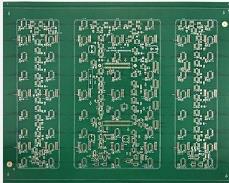
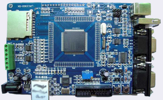
The number of layers of the PCB poard means that there are several independent wiring layers. Usually the number of layers is even and contains the two outermost layers. Most motherboards have 4 to 8 layers of structure, but technically it is possible to achieve nearly 100 layers of PCB boards. Most large supercomputers use fairly multi-layered motherboards, but because these types of computers can already be replaced by clusters of many ordinary computers, super-multilayered boards have gradually ceased to be used. Because the layers in the PCB are tightly integrated, it is generally not easy to see the actual number, but if you look closely at the motherboard, you may be able to see it.
The automatic detection technology of circuit boards has been applied with the introduction of surface mount technology, and the packaging density of circuit boards has increased rapidly. Therefore, even for low-density and average-number circuit boards, the automatic detection of circuit boards is not only basic, but also economical. In complex circuit board inspection, two common methods are the needle bed test method and the double probe or flying probe test method.