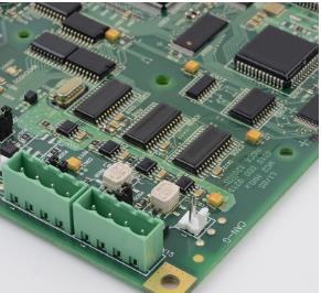
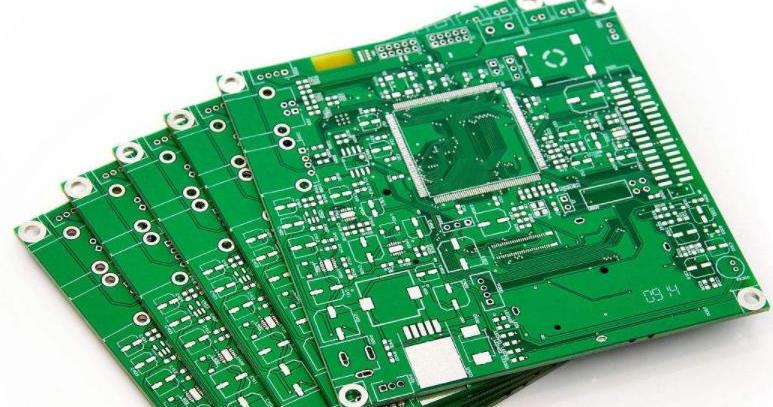
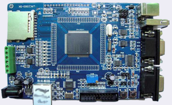
Due to the increase in the packaging density of integrated circuits, a high concentration of interconnection lines has resulted, which necessitates the use of multiple substrates. In the layout of printed circuits, unforeseen design problems such as noise, stray capacitance, and crosstalk have appeared. Therefore, the printed circuit board design must focus on minimizing the length of the signal line and avoiding parallel routes. Obviously, in single-panel, or even double-panel, these requirements cannot be satisfactorily answered due to the limited number of crossovers that can be achieved. In the case of a large number of interconnection and crossover requirements, to achieve a satisfactory performance of the circuit board, the board layer must be expanded to more than two layers, thus a multilayer circuit board has appeared. Therefore, the original intention of manufacturing multi-layer circuit boards is to provide more freedom for selecting appropriate wiring paths for complex and/or noise-sensitive electronic circuits. Multilayer circuit boards have at least three conductive layers, two of which are on the outer surface, and the remaining layer is integrated into the insulating board. The electrical connection between them is usually achieved through plated through holes on the cross section of the circuit board. Unless otherwise specified, multi-layer printed circuit boards, like double-sided boards, are generally plated through-hole boards.

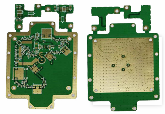
Multi-substrates are manufactured by stacking two or more circuits on top of each other, and they have reliable pre-set interconnections. Since drilling and plating have been completed before all the layers are rolled together, this technique violates the traditional manufacturing process from the beginning. The two innermost layers are composed of traditional double panels, while the outer layers are different, they are composed of independent single panels. Before rolling, the inner substrate will be drilled, through-hole plating, pattern transfer, development and etching. The outer layer to be drilled is the signal layer, which is plated through in such a way as to form a balanced copper ring on the inner edge of the through hole. The layers are then rolled together to form a multi-substrate, which can be connected to each other (between components) using wave soldering.
Rolling may be done in a hydraulic press or in an overpressure chamber (autoclave). In the hydraulic press, the prepared material (for pressure stacking) is placed under cold or preheated pressure (the material with high glass transition temperature is placed at a temperature of 170-180°C). The glass transition temperature is the temperature at which an amorphous polymer (resin) or part of the amorphous region of a crystalline polymer changes from a hard, rather brittle state to a viscous, rubbery state.
Multi-substrates are put into use in professional electronic equipment (computers, military equipment), especially when weight and volume are overloaded. However, this can only be achieved by increasing the cost of multiple substrates in exchange for an increase in space and a reduction in weight. In high-speed circuits, multi-substrates are also very useful. They can provide designers of printed circuit boards with more than two layers of board surfaces to lay wires and provide large grounding and power supply areas.