Another difficulty in modern mixed-signal PCB design is that there are more and more different digital logic devices, such as GTL, LVTTL, LVCMOS and LVDS logic. The logic threshold and voltage swing of each logic circuit are different, but these different logic thresholds The circuit with the voltage swing must be designed together on a PCB. Here, through thorough analysis of high-density, high-performance, mixed-signal PCB layout and wiring design, you can master successful strategies and technologies.
Basics of mixed-signal circuit wiring
When digital and analog circuits share the same components on the same board, the layout and wiring of the circuit must be methodical.
In the mixed-signal PCB design, there are special requirements for power supply wiring, and the analog noise and digital circuit noise are required to be isolated from each other to avoid noise coupling. As a result, the complexity of layout and wiring increases. The special requirements for power transmission lines and the requirement to isolate noise coupling between analog and digital circuits have further increased the complexity of the layout and wiring of mixed-signal PCBs.
If the power supply of the analog amplifier in the A/D converter and the digital power supply of the A/D converter are connected together, it is likely to cause the mutual influence of the analog part and the digital part of the circuit. Perhaps, due to the location of the input/output connectors, the layout scheme must mix the wiring of digital and analog circuits.
Before layout and routing, engineers must figure out the basic weaknesses of the layout and routing scheme. Even with false judgments, most engineers tend to use layout and wiring information to identify potential electrical effects.
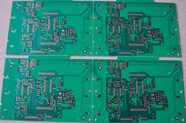
The following will illustrate the technology of mixed-signal PCB layout and routing through the design of the OC48 interface card. OC48 stands for Optical Carrier Standard 48, which is basically oriented to 2.5Gb serial optical communication. It is one of the high-capacity optical communication standards in modern communication equipment. The OC48 interface card contains several typical mixed-signal PCB layout and wiring problems. The layout and wiring process will specify the sequence and steps to solve the mixed-signal PCB layout scheme.
The OC48 card contains an optical transceiver that realizes the bidirectional conversion of optical signals and analog electrical signals. Analog signal input or output digital signal processor, DSP converts these analog signals into digital logic levels, which can be connected with microprocessor, programmable gate array, DSP and microprocessor system interface circuit on OC48 card . The independent phase-locked loop, power filter and local reference voltage source are also integrated.

Among them, the microprocessor is a multi-power device, the main power is 2V, and the 3.3V I/O signal power is shared by other digital devices on the board. Independent digital clock source provides clock for OC48 I/O, microprocessor and system I/O.
After checking the layout and wiring requirements of different functional circuit blocks, a 12-layer board is initially recommended. The configuration of the microstrip and stripline layers can safely reduce the coupling of adjacent wiring layers and improve impedance control. A grounding layer is set between the first and second layers to isolate the wiring of sensitive analog reference sources, CPU cores and PLL filter power supplies from the microprocessor and DSP devices on the first layer. The power and ground planes always appear in pairs, the same as what was done on the OC48 card for the shared 3.3V power plane. This will reduce the impedance between the power supply and ground, thereby reducing the noise on the power signal.
Avoid running digital clock lines and high-frequency analog signal lines near the power plane, otherwise, the noise of the power signal will be coupled to the sensitive analog signal.
According to the needs of digital signal wiring, carefully consider the use of power and analog ground plane openings (split), especially at the input and output ends of mixed-signal devices. Passing through an opening in the adjacent signal layer will cause impedance discontinuity and poor transmission line loops. These will cause signal quality, timing and EMI issues.
Sometimes adding several ground layers, or using several outer layers for the local power layer or ground layer under a device, can eliminate the opening and avoid the above problems. Multiple ground layers are used on the OC48 interface card. Maintaining the stacking symmetry of the position of the opening layer and the wiring layer can avoid card deformation and simplify the manufacturing process. Since 1 ounce of copper clad laminates are highly resistant to large currents, 1 ounce of copper clad laminates should be used for the 3.3V power layer and the corresponding ground layer, and 0.5 ounces of copper clad laminates can be used for other layers. This can reduce transient high currents or spikes caused by Voltage fluctuations.
If you design a complex system from the ground plane up, you should use cards with a thickness of 0.093 inches and 0.100 inches to support the wiring layer and the ground isolation layer. The thickness of the card must also be adjusted according to the size of the via pad and the wiring feature of the hole, so that the aspect ratio of the hole diameter to the thickness of the finished card does not exceed the aspect ratio of the metallized hole provided by the manufacturer.
If you want to design a low-cost, high-yield commercial product with the least number of wiring layers, you must carefully consider the wiring details of all special power supplies on the mixed-signal PCB before layout or wiring. Before starting layout and routing, let the target manufacturer review the preliminary layering plan. Basically, the layering should be based on the thickness of the finished product, the number of layers, the weight of copper, the impedance (with tolerance), and the size of the smallest via pads and holes. The manufacturer should provide a written layering recommendation.
The proposal should include all configuration examples of controlled impedance stripline and microstrip line. You need to combine your impedance prediction with the manufacturer's impedance. Then, use these impedance predictions to verify the signal routing characteristics in the simulation tool used to develop CAD routing rules.
OC48 card layout
The high-speed analog signal between the optical transceiver and the DSP is very sensitive to external noise. Similarly, all special power supply and reference voltage circuits also cause a lot of coupling between the analog and digital power transmission circuits of the card. Sometimes, limited by the shape of the chassis, a high-density board has to be designed. Due to the high position of the external optical cable access card and the relatively high component size of the optical transceiver, the position of the transceiver in the card is largely fixed. The system I/O connector position and signal distribution are also fixed. This is the basic work that must be completed before layout.
Like most successful high-density analog layout and routing schemes, the layout must meet the routing requirements, and the layout and routing requirements must be balanced. For the analog part of a mixed-signal PCB and a local CPU core with a 2V operating voltage, it is not recommended to use the "layout before wiring" method. For the OC48 card, the DSP analog circuit part including the analog reference voltage and the analog power supply bypass capacitor should be interactively wired first. After completing the wiring, the entire DSP with analog components and wiring should be placed close enough to the optical transceiver to fully ensure the shortest wiring length, bending and vias from the high-speed analog differential signal to the DSP. The symmetry of the differential layout and routing will reduce the impact of common mode noise. However, it is difficult to predict the best plan for the layout before routing.
Consult the chip distributor for design guidelines for PCB layout. Before designing in accordance with the guidelines, it is necessary to fully communicate with the distributor's application engineer. Many chip distributors have strict time constraints on providing high-quality layout recommendations. Sometimes, the solutions they provide are feasible for "first-level customers" who use the device. In the field of signal integrity (SI) design, the signal integrity design of new devices is particularly important. According to the distributor’s basic guidelines and combined with the specific requirements of each power and ground pin in the package, you can begin to lay out and route the OC48 card with integrated DSP and microprocessor.