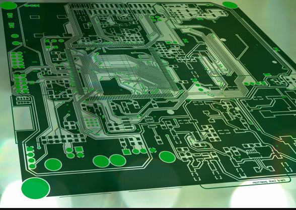
1. How to choose PCB board?
The choice of PCB board must strike a balance between meeting design requirements and mass production and cost. The design requirements include both electrical and mechanical parts. Usually, this material problem is more important when designing very high-speed PCB boards (frequency greater than GHz). For example, the commonly used FR-4 material, the dielectric loss at a frequency of several GHz will have a great influence on the signal attenuation, which may not be suitable. As far as electricity is concerned, pay attention to whether the dielectric constant and dielectric loss are suitable for the designed frequency.
2. How to avoid high frequency interference?
The basic idea of avoiding high-frequency interference is to minimize the electromagnetic field interference of high-frequency signals, which is the so-called crosstalk (Crosstalk). Can increase the distance between high-speed signal and analog signal, or add groundguard/shunttraces beside the analog signal. Also pay attention to the noise interference from the digital ground to the analog ground.
3. How to solve the signal integrity problem in high-speed PCB design?
Signal integrity is basically a problem of impedance matching. The factors that affect impedance matching include the structure and output impedance of the signal source, the characteristic impedance of the trace, the characteristics of the load end, and the topology of the trace. The solution is to rely on the topology of termination and adjustment of the wiring.

4. Can a ground wire be added to the middle of the differential signal line?
It is generally not possible to add a ground wire in the middle of the differential signal. Because the most important point of the application principle of differential signals is to use the benefits of coupling between differential signals, such as flux cancellation and noise immunity. If you add a ground wire in the middle, it will destroy the coupling effect.
5. Is it necessary to add ground wire shields on both sides when fabricating the clock?
Whether to add a shielded ground wire or not depends on the crosstalk/EMI situation on the board, and if the shielded ground wire is not handled well, it may make the situation worse.
6. Which end of the AC coupling on the high-speed signal on the PCB is better?
We often see different processing methods, some near the receiving end and some near the transmitting end. Let us first look at the role of AC coupling capacitors. There are three points: 1. source and sink terminals have different DCs, so DC is blocked; 2. DC components may be crosstalked during signal transmission, so DC blocking makes the signal eye diagram better; 3. AC coupling Capacitors can also provide protection against DC bias and overcurrent. After all, the role of the AC coupling capacitor is to provide a DC bias, filter out the DC component of the signal, and make the signal symmetrical about the 0 axis. So why add this AC coupling capacitor, of course, is beneficial. Increasing the AC coupling capacitor will definitely enable better communication between the two stages and improve the noise tolerance. It is important to know that AC coupling capacitors are generally the point where high-speed signal impedance is discontinuous and will cause the signal edge to become slow.
So, the answer is also very clear:
1) Some agreements or manuals will provide design requirements, and we will place them in accordance with the designguideline requirements. 2) There is no requirement of Article 1, if it is from IC to IC, please place it close to the receiving end. 3) If it is an IC to a connector, please place it close to the connector.
7. How to check whether the PCB meets the design process requirements before leaving the factory?
Many PCB manufacturers have to go through a power-on network continuity test before the PCB processing is completed to ensure that all connections are correct. At the same time, more and more manufacturers are also using x-ray testing to check some failures during etching or lamination. For finished boards after patch processing, ICT testing is generally used, which requires ICT test points to be added during PCB design. If there is a problem, you can also use a special X-ray inspection equipment to rule out whether the processing causes the fault.