Abstract: The emergence of lead-free PCB poses new problems for in-circuit testing (ICT). This article describes the existing PCB surface treatment processes and analyzes the impact of these processes on ICT. It is pointed out that the key to ICT is *** *Reliability of contact with test points, and introduces the specific changes that need to be made during the PCB construction process to meet ICT requirements.
ICT still plays an important role in the manufacturing and testing process of printed circuit board assembly (PCA), but how will people's pursuit of lead-free PCB affect the ICT stage?
This article will talk about the surface treatment of lead-free PCB, especially in the ICT stage of the manufacturing process, and reveal that the successful test of lead-free surface treatment also depends on the beneficial contribution of the PCB construction process.
PCB surface treatment process selection
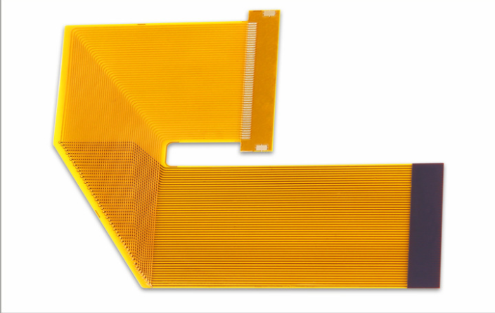
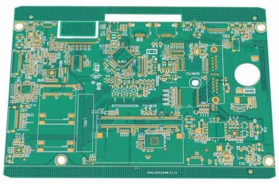
Before we understand the cause and effect, it is very important to describe the types of PCB surface treatment processes available and what these types can provide. All printed circuit boards (PCBs) have a copper layer on the board. If the copper layer is not protected, it will be oxidized and damaged. There are many different protective layers available, the most common ones are hot air solder leveling (HASL), organic solder protection (OSP), electroless nickel-gold immersion (ENIG), silver immersion, and tin immersion.

Hot Air Solder Leveling (HASL)
HASL is the main lead surface treatment process used in the industry. The process is formed by immersing the circuit board in a lead-tin alloy, and the excess solder is removed by an "air knife". The so-called air knife is hot air blowing on the surface of the board. For the PCA process, HASL has many advantages: it is the cheapest PCB, and the surface layer can be soldered after multiple reflow soldering, cleaning and storage. For ICT, HASL also provides a process for automatically covering test pads and vias with solder. However, compared with the existing alternative methods, the flatness or coplanarity of the HASL surface is poor. Now there are some lead-free HASL alternative processes, which are becoming more and more popular due to the natural replacement characteristics of HASL. For many years, HASL has been applied with good results, but with the emergence of "environmental protection" green process requirements, the existence of this process is numbered. In addition to the lead-free problem, increasing board complexity and finer pitch have exposed many limitations of the HASL process.
Advantage: The lowest cost PCB surface technology, maintains solderability throughout the manufacturing process, and has no negative impact on ICT.
Disadvantages: Usually lead-containing processes are used. Lead-containing processes are now restricted and will eventually be eliminated by 2007. For fine pin pitch (<0.64mm), it may cause solder bridging and thickness problems. The uneven surface can cause coplanarity problems in the assembly process.
Organic Solder Protector
Organic Solder Protector (OSP) is used to produce a thin, uniform protective layer on the copper surface of the PCB. This coating protects the circuit from oxidation during storage and assembly operations. This process has been around for a long time, but only recently has it gained popularity as lead-free technology and fine-pitch solutions are sought.
Using OSP surface treatment, if the test point is not welded, it will cause the contact problem of the needle bed fixture in the ICT. Merely changing to a sharper **** type to pass through the OSP layer will only cause damage and puncture the PCA test vias or test pads. Studies have shown that switching to a higher detection force or changing the **** type has little effect on the yield. Untreated copper has an order of magnitude higher yield strength than leaded solder, and the only result is that it will damage the exposed copper test pad. All testability guidelines strongly recommend not to directly probe exposed copper. When using OSP, it is necessary to define a set of OSP rules for the ICT phase. The most important rule requires that the Stencil be opened at the beginning of the PCB process to allow solder paste to be applied to the test pads and vias that need to be contacted by the ICT.
Advantages: Comparable with HASL in unit cost, good coplanarity, lead-free process, and improved solderability.
Silver Immersion
Silver immersion is a newly added method of PCB surface treatment. It is mainly used in Asia and is being promoted in North America and Europe. During the soldering process, the silver layer melts into the solder joints, leaving a tin/lead/silver alloy on the copper layer. This alloy provides a very reliable solder joint for BGA packages. Its contrasting color makes it easy to be inspected, and it is also a natural alternative to HASL in welding.
Silver immersion is a surface processing technology with very good development prospects, but like all new surface processing technologies, end users are very conservative. Many manufacturers regard this process as a "under investigation" process, but it is likely to become the best lead-free surface process choice.
Advantages: good weldability, smooth surface, natural replacement of HASL immersion.
Disadvantages: The conservative attitude of end users means that there is a lack of relevant information in the industry.
tin immersion
This is a relatively new surface treatment process, which has many similar characteristics to the silver immersion process. However, due to the need to prevent thiourea (which may be a carcinogen) used in the tin immersion process in the PCB manufacturing process, there are major health and safety issues that need to be considered. In addition, attention should be paid to tin migration ("tin burr" effect), although anti-migration chemicals can achieve a certain effect in controlling this problem.
Advantages: good weldability, smooth surface, relatively low cost.
Disadvantages: health and safety issues, limited number of thermal cycles.
The above is the main method of PCB lead-free processing. HASL will still be the most widely used PCB processing technology. In this case, there will be no change for test engineers. In some countries, HASL has been banned by law and alternatives have been adopted. As PCA manufacturing expands to more and different global regions, there will be more and more lead-free processing processes that can be seen in ICT testing. Although OSP is not a natural alternative to HASL, it has become the preferred alternative treatment solution studied by PCA manufacturers. When the process is not changed to allow solder paste to be used on the test pads and vias, this will cause actual ICT test reliability issues
The conclusion is that the process of PCB surface treatment is not perfect, and each method has its own issues that need to be considered. Some of these problems are more serious than others, and all these lead-free PCB surface treatment processes need to be modified in the process steps to prevent fixture contact reliability problems in ICT.
The direct detection of the copper surface combined with the higher force required to penetrate the OSP layer creates the actual potential threat of damaging the thin copper layer and causing an internal short circuit. Therefore, our recommendation is to never probe exposed copper surfaces. Recent examples have shown that after 5 to 10 fixture excitations, board vias or test points may be punctured.
For some PCA manufacturers, the impact of OSP on ICT has caused such a big problem that they no longer use OSP at all. Other manufacturers began to learn how to follow the "OSP rules" listed below. "OSP Rules" for ICT test fixtures and procedures: Pay attention to the latest industry testability recommendations, such as www.smta.org. -Always add solder paste to the test connection point (test pad or via), and do not probe the exposed copper layer covered by the OSP.
It seems that the trend of some PCB companies is that OSP is considered a natural alternative to HASL. This choice is probably due to the recognition of unit cost savings. ICT engineers should pay attention to this trend: OSP-plated PCBs will not achieve the performance of other optional lead-free surface treatment processes, unless the test pad is covered by solder.