What are the raw materials of PCB (Printed Circuit Board)? "Glass fiber", this kind of material can be seen in daily life. For example, the core of fireproof cloth and fireproof felt is glass fiber. Glass fiber is easy to combine with resin, so that the tightly structured and high-strength glass fiber cloth is immersed in the resin. After hardening, a heat-insulating, non-flexible PCB substrate is obtained-if the PCB is broken, the edges are whitened and layered, which is enough to prove that the material is resin glass fiber.
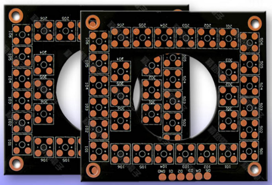
The insulating board alone cannot transmit electrical signals, so it is necessary to coat the surface with copper. In the factory, the code name of the common copper-clad substrate is FR-4, which is generally the same among various board and card manufacturers. Of course, if it is a high-frequency board, it is best to use a higher-cost copper-clad PTFE Glass cloth laminate. The copper-clad process is very simple. Generally, it can be manufactured by rolling and electrolysis. The so-called rolling is to paste high-purity (>99.98%) copper on the PCB substrate by rolling-because epoxy resin and copper foil are excellent The adhesiveness of copper foil, the adhesion strength of copper foil and the high working temperature, can be dip-soldered in molten tin at 260°C without blistering. This process is quite like rolling a dumpling wrapper, but the dumpling wrapper is very thin and thin, the thinnest can be less than 1mil (industrial unit: mil, which is one thousandth of an inch, equivalent to 0.0254mm)! Usually the factory has very strict requirements on the thickness of copper foil, generally between 0.3 mil and 3 mil, and there is a dedicated copper foil thickness tester to test its quality. The copper coating on PCBs used by old radios and amateurs is very thick, which is far inferior to the quality in computer board factories.

Why should the copper foil be so thin? It is mainly based on two reasons: one is that a uniform copper foil can have a very uniform temperature coefficient of resistance and a low dielectric constant, which can make the signal transmission loss smaller. This is different from the capacitor requirement, which requires a high dielectric constant. In order to accommodate a higher capacity in a limited volume, why the capacitor is smaller than the aluminum capacitor, in the final analysis, the dielectric constant is high. Secondly, the temperature rise of thin copper foil is small under the condition of large current, which has great benefits for heat dissipation and component life. It is also the reason that the copper wire width in digital integrated circuits should be less than 0.3cm. The well-made PCB finished board is very uniform and has a soft gloss (because the surface is brushed with solder resist), which can be seen with the naked eye.
Next, we will use the copper etching solution (chemicals that corrode copper) to etch the substrate. The copper without dry film protection is completely covered, and the circuit diagram under the hardened dry film is displayed on the substrate. This whole process is called "image transfer", which occupies a very important position in the PCB manufacturing process. Naturally, the next step is to make a multilayer board! According to the above steps, the production is only a single panel, even if the two sides are processed, it is only a double panel, but we can often find that the board in our hands is a four-layer board or a six-layer board (or even an 8-layer board). How exactly is this made? ?
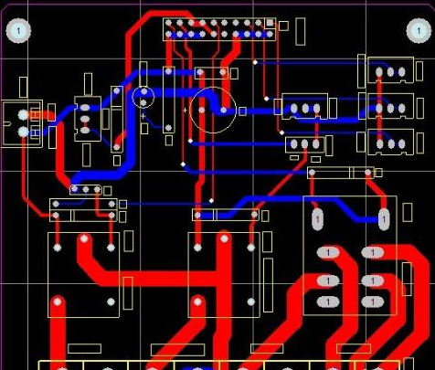
With the above foundation, it is actually not difficult to understand, just make two double panels and "stick" them together! For example, if we make a typical four-layer board (divided into 1 to 4 layers in order, 1/4 is the outer layer, signal layer, 2/3 is the inner layer, ground and power layer), first do 1/2 respectively And 3/4 (the same substrate), and then glue the two substrates together. However, this adhesive is not an ordinary glue, but a resin material in a softened state. Firstly, it is insulating, and secondly, it is very thin and has good adhesion to the substrate. We call it PP material, and its specifications are the thickness and the amount of glue (resin). Of course, generally four-layer and six-layer boards are invisible to us, because the thickness of the substrate of the six-layer board is relatively thin. How much thickness can the four-layer board of the base plate increase? The thickness of the board has a certain specification, otherwise it will not be inserted into various card slots. At this point, readers will have questions again, don't the signals between the multilayer boards need to be conducted? Now that PP is an insulating material, how to realize the interconnection between layers? Don't worry, we need to drill holes before bonding the multilayer boards! After drilling a hole, you can align the corresponding copper wires at the upper and lower positions of the circuit board, and then let the hole wall with copper. Isn't it equivalent to a wire connecting the circuit in series? We call this type of hole a via. These holes need to be drilled by a drilling machine. Modern drilling machines can drill very small holes and very shallow holes. There are hundreds of holes of different sizes and depths on a motherboard. We use high-speed drilling machines. It will take at least an hour to drill. After drilling the hole, we then conduct hole plating (this technology is called Plated-Through-Hole technology, PTH) to make the hole conductive.
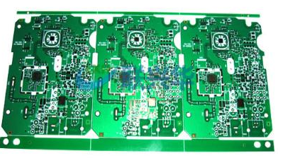
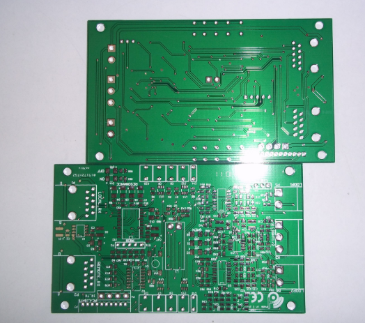
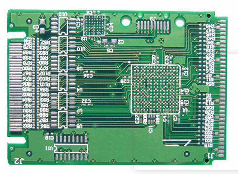
Motherboard production requires a lot of soldering. If you solder directly, it will have two serious consequences: 1. The copper wire on the board surface is oxidized and cannot be welded; 2. The overlap welding phenomenon is serious-because the distance between the wires is too small. NS. Therefore, we must coat the entire PCB substrate with a layer of armor-this is the solder resist, which is commonly known as the solder resist. It has no affinity for liquid solder, and will be affected by the light of a specific spectrum. It changes and hardens. This feature is similar to dry film. The color of the board we see is actually the color of the solder mask. If the solder mask is green, then the board is green. Everyone knows how the corresponding colors come from. Bar? Finally, don’t forget the screen printing, gold finger plating (for graphics cards or PCI cards) and quality inspection to test whether the PCB has a short circuit or open circuit. You can use optical or electronic testing. The optical method uses scanning to find the defects in each layer, and the electronic test usually uses a flying-probe to check all connections. Electronic testing is more accurate in finding short circuits or open circuits, but optical testing can more easily detect incorrect gaps between conductors. To sum up, the production process of a typical PCB factory is as follows: blanking - inner layer production - pressing - drilling - copper plating - outer layer production - solder resist printing - text printing - surface treatment - shape processing.