The electronics industry is striving to recover from the economic crisis, and the pressure to provide comprehensive support for the process from design to manufacturing is also increasing. Electronic companies around the world have to bring differentiated products to the market at a faster speed and lower cost, and this trend will continue due to economic weakness. Even in China's PCB market, system design and manufacturing support tools urgently need to utilize the latest technology to increase productivity.
In a survey conducted by the Aberdeen Group, many leading electronics companies identified six design technology best practices that can actively meet business goals. With the slow recovery of the economic situation, these basic PCB technology practices will become an essential part of the development of companies in 2012.
The following is an overview of these 6 key strategies to make the company's work smarter. We believe these strategies will become the key to development in 2012.
Technical Strategy 1: Product collaborative development process
Collaboration usually refers to the ability to turn serial operations into parallel, and has two modes. The first is the ability to allow multiple designers to work in the same design process at the same time. This approach is not new, but the effectiveness of the new technology is vastly different from the original one. The designer can always manipulate the PCB design database and split it. Then every designer works in the design process-but in the end the database must be re-merged. The merging process is very time-consuming and error-prone, but the end result can shorten the design cycle.

"The future plan is to simulate in software, such as a virtual prototype."
At present, we have the ability to let multiple designers work in the same database at the same time, without the need to split the database. This is suitable for many processes in PCB design, including schematic input, constraint (high-speed and manufacturing rules) input and management, and physical layout. In addition, every designer can see the results of his colleagues' operations in real time. This not only significantly shortens the design cycle time, but also improves the designer's productivity and product quality. Some users of this technology report saving 30 to 70% of design time. In order to remain competitive in 2012, companies must achieve similar design cycle improvements).
Technical Strategy 2: Virtual Prototype
Usually companies validate their products by building and testing multiple prototypes. Design a PCB, build a physical prototype, test it in the lab, determine what changes need to be made, redesign, and repeat the related process.
There are several problems with this method. First, it is time-consuming and expensive to build and debug a prototype. If the time to market is very tight, it is likely to miss the market opportunity. Second, testing in the laboratory may not find all potential problems. For example, you want the product to be used in harsh environments such as severe vibration for many years, but the "vibration and heat treatment" laboratory may not be able to run long enough to find long-term problems. Similarly, signal integrity also has this problem. Extreme critical conditions are likely to be unavailable in the laboratory.
The solution in the future is to simulate in software, such as a virtual prototype. This operation can be performed in the PCB design process and will cover many possible areas: signal (digital, analog, radio frequency) and power network integrity; thermal management in integrated circuits, packaging, PCB and full system simulation; vibration and shock (Figure 2); PCB manufacturing and assembly practices; 3D mechanical interface, etc. Execution in the entire design process can ensure that the design continues without backup and correction. In addition, the software can detect extreme critical conditions and can simulate problems in the laboratory for weeks and months in a matter of hours. Although designers like to get the physical object as quickly as possible, and the implementation of a wide range of virtual prototypes may be delayed, the latter can shorten the cycle, reduce costs, and improve the designer's productivity and product quality/reliability.
Technical Strategy 3: Process support from design to manufacturing
Time to market and product cost are the key to many industries. Even in the military/aerospace and automotive industries, which in the past faced restrictions on longer development times and/or high costs, they now have more aggressive goals for this issue. In addition, PCB designers must not forget that even if data enters the manufacturing process, their responsibilities have not yet ended. At the same time, from the perspective of EDA suppliers, the important thing is that support is not to the end of the design phase, not to allow designers to easily fulfill their responsibilities for manufacturable products, but to work with manufacturers to optimize their production lines to achieve the lowest cost products. deliver.
Once the design enters the manufacturing process through an intelligent interface, such as ODB++, the manufacturer can use the software to model the production line and optimize its use. While the production line is running, the software will continuously monitor issues such as on-time delivery of parts, machine downtime, and product traceability. Even if a quality defect occurs, it can ensure that equipment or processes with a failure rate below the acceptable failure rate are tracked and highlighted.
Technology Strategy 4: Complexity Management
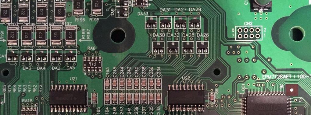
For differentiated products that beat competitors, the company must use the latest and most advanced technology to compress more functions into a smaller space while still satisfying the positive market opportunities. This will become even more important in 2012. Integrated circuit technology continues to improve in terms of high density, high speed, more pins in a smaller space, and higher power consumption. PCB (printed circuit board) manufacturing technology, such as HDI/microvia technology, can increase density, but the design is also more complicated. Faced with this ever-increasing complexity, how can we maintain and increase designer productivity? The answer is to also increase the functionality of design tools.
Technology Strategy 5: Interdisciplinary Cooperation
Product development and delivery require interdisciplinary cooperation. In the electronics field, we have experts in integrated circuits, packaging, FPGA, RF, analog and digitalization; in the mechanical field, we have engineers who design enclosures and perform CAE analysis; we have procurement, supply chain and manufacturing personnel; we have Embedded software development. All of these require effective cooperation in the development process. In the past, it was done through paper and e-mail, but now it is mainly through electronic media, but there are still problems with transferring large amounts of data between team members. How can you effectively determine what changes have occurred, how to respond in your field, and what controls have you actually adopted? Such issues must be dealt with in the near future.
In fact, most interactions are a negotiation. For example, if a mechanical engineer finds that a component on the PCB will interfere with the physical product housing, the engineer can propose to replace the component's location. This will take the form of a gradual (only when replacement) proposal is communicated to the PCB designer-unlike a large amount of data transfer, the PCB designer must be sorted to determine the proposal. Recently, progressive change performance has been developed into a standard ("EDMD") by Mentor Graphics, PTC and users, and has been approved by ProSTEP.
The proposal will be shown to the PCB designer in the form of graphics, and the latter will accept, reject or make a proposal that is more suitable for this PCB based on the actual situation of the PCB. The negotiation process will continue until agreement is reached, at which time both the mechanical and electrical databases will be updated. This fully electronic collaboration is just one of many examples of actual operations.
Technology Strategy 6: Intellectual Property (IP) Management
Finally, first-class electronics companies determine that the key to future success lies in their work processes and database management.
Design team members, whether they are located locally or scattered around the world, need to create an effective authority and strictly manage the assets that the company considers the most important. The company's database administrator enters the information of the qualified components into the approved management infrastructure, which can be evaluated by the designer. All or part of the pre-designed PCB can be added to the library for reuse in future projects.
As the PCB design progressed, the team created schematics, constraints, and PCB layout data. The data management of this work process is very complicated, and an infrastructure system for managing electronic intellectual property (IP) needs to be created specifically. Data edited by different team members will face version management and synchronization issues. Companies can hire service organizations to design some products and hope to share only some of their IP. This is to eliminate the complexity of using standard PLM systems.