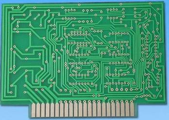
1.From the schematic to the PCB design process Establish component parameters -> input principle netlist -> design parameter settings -> manual layout -> manual wiring -> verify design -> review -> CAM output.
2.Parameter setting The distance between adjacent wires must be able to meet the electrical safety requirements, and in order to facilitate operation and production, the distance should be as wide as possible. The minimum spacing must be at least suitable for the voltage tolerated.When the wiring density is low, the spacing of the signal lines can be increased appropriately. For signal lines with a large gap between high and low levels, the spacing should be as short as possible and the spacing should be increased. Generally, Set the trace spacing to 8mil. The distance between the edge of the inner hole of the pad and the edge of the printed board should be greater than 1mm,which can avoid the defects of the pad during processing. When the traces connected to the pads are thin, the connection between the pads and the traces should be designed into a drop shape.The advantage of this is that the pads are not easy to peel, but the traces and the pads are not easily disconnected.

3.The component layout practice has proved that even if the circuit schematic is designed correctly and the printed circuit board is not designed properly, it will adversely affect the reliability of electronic equipment. For example, if the two thin parallel lines of the printed board are close together, the signal waveform will be delayed and reflected noise will be formed at the terminal of the transmission line. The performance drops, so when designing the printed circuit board, you should pay attention to adopting the correct method. Each switching power supply has four current loops.
4.Wiring The switching power supply contains high-frequency signals. Any printed line on the PCB can function as an antenna. The length and width of the printed line will affect its impedance and inductance, thereby affecting the frequency response. Even printed lines that pass DC signals can couple to radio frequency signals from adjacent printed lines and cause circuit problems (and even radiate interfering signals again). Therefore, all printed lines that pass AC current should be designed to be as short and wide as possible, which means that all components connected to the printed lines and other power lines must be placed very close. The length of the printed line is proportional to its inductance and impedance, and the width is inversely proportional to the inductance and impedance of the printed line. Length reflects the wavelength of the printed line's response. The longer the length, the lower the frequency at which the printed line can send and receive electromagnetic waves, and it can radiate more radio frequency energy. According to the current of the printed circuit board, try to increase the width of the power line to reduce the loop resistance. At the same time, make the direction of the power line and the ground line consistent with the direction of the current, which helps to enhance the anti-noise ability. Grounding is the bottom branch of the four current loops of the switching power supply. It plays a very important role as a common reference point for the circuit. It is an important method to control interference. Therefore, the placement of the grounding wire should be carefully considered in the layout. Mixing various groundings will cause unstable power supply operation.
5.After the wiring design is completed, it is necessary to carefully check whether the wiring design complies with the rules set by the designer. At the same time, it is also necessary to confirm whether the rules set meet the requirements of the printed board production process. Generally check the wire and wire, wire and component welding Whether the distance between the disk, the wire and the through hole, the component pad and the through hole, and the distance between the through hole and the through hole is reasonable, and whether it meets the requirements of PCB production. Whether the width of the power line and the ground line are appropriate, and whether there is a place to widen the ground line in the PCB. Note: Some errors can be ignored. For example, when a part of the outline of some connectors is placed outside the board frame, errors will occur when checking the spacing; in addition, each time the traces and vias are modified, the copper must be re-plated.
6.Review According to the "PCB checklist", the content includes design rules, layer definitions, line widths, spacing, pads, and via settings. It should also focus on reviewing the rationality of the device layout, the routing of power and grounding networks, and high-speed The routing and shielding of the clock network, the placement and connection of decoupling capacitors, etc.
Seven.
Design output Matters needing attention when outputting Gerber files:
a.The layers that need to be output include wiring layer (bottom layer), silk screen layer (including top silk screen, bottom silk screen), solder mask (bottom solder mask), drilling layer (bottom layer), and a drilling file (NC Drill) )
b.When setting the Layer of the silk screen layer, do not select Part Type, select the top (bottom layer) and Outline, Text, and Line of the silk screen layer. When setting the Layer of each layer, select the Board Outline.When setting the Layer of the silk screen layer, Don't choose Part Type, choose Outline, Text, Line of the top layer (bottom layer) and silk screen layer. d. When generating drilling files,use the default settings of PowerPCB and do not make any changes.