The revival of PCB testing technology is an inevitable result of the miniaturization of surface mount devices and circuit boards. Once any system is so small that it is difficult to detect the inside of the base, there are only some input and output channels that interact with the outside of the system, and this is where the function test comes in.
This situation is exactly the same as in the early days of functional testing development thirty or forty years ago. However, unlike the past, today’s international standards for functional test instruments (such as PXI, VXI, etc.) have gradually matured, and standard instrument modules and virtual instrument software technologies have been commonly used, which greatly increases the versatility and versatility of future functional test instruments. Flexibility and help reduce costs. At the same time, the testability design results of the circuit board, and even the testability design results of the super-large-scale hybrid integrated circuit may be transplanted to the functional test technology. Using the standard interface of the boundary scan technology and the corresponding testability design, the functional tester can be used to program the system online just like the online test equipment. Undoubtedly, the functional tester of the future will tell us much more information than the judgment of "qualified or unqualified".
Surface mount devices and circuits have been in an endless process of miniaturization, and relentlessly drive the elimination and evolution of some related test technologies. Under the evolutionary pressure of the miniaturization of electronic products, technology, like a species, follows the simple rule of "survival of the fittest". Paying attention to the development of test technology can help us predict the future.
Since the surface mount technology (SMT) began to gradually replace the jack-type mounting technology, the devices mounted on the circuit board have become smaller and smaller, and the functions contained in the unit area on the board have become more and more powerful.

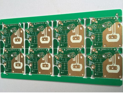
As far as passive surface mount devices are concerned, 0805 devices, which were widely used ten years ago, are used today only about 10% of the total number of similar devices; and the amount of 0603 devices has begun to decline four years ago., Replaced by 0402 devices. At present, even smaller 0201 devices are gaining momentum. It took about ten years to switch from 0805 to 0603. Undoubtedly, we are in an era of accelerated miniaturization. Let's look at surface-mounted integrated circuits. From the quad flat package (QFP) that dominated ten years ago to today’s chip flip-chip (FC) technology, a wide variety of package forms have emerged, such as thin small lead package (TSOP), ball array package (BGA), Micro Ball Array Package (μBGA), Chip Scale Package (CSP), etc. Looking at the evolution of chip packaging technology, its main feature is that the surface area and height of the device are significantly reduced, while the pin density of the device is rapidly increasing. In terms of a chip with the same logic function complexity, the area occupied by the flip-chip device is only one-ninth of the area occupied by the original quad flat package device, and the height is only about one-fifth of the original.
Miniature packaged components and high-density PCB bring new challenges to testing
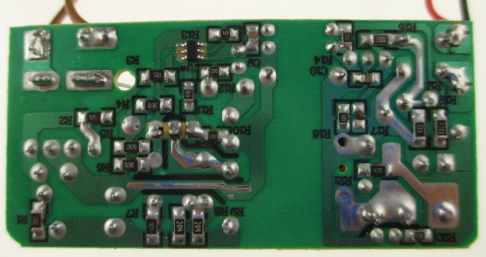
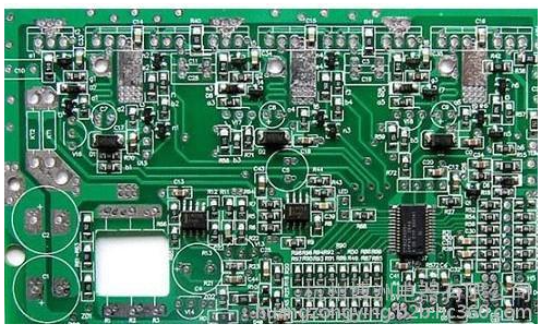
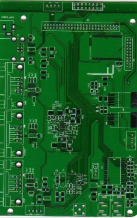
The continuous shrinking of the size of surface mount devices and the subsequent high-density circuit installation have brought great challenges to the test. The traditional manual visual inspection is unsuitable even for circuit boards of medium complexity (such as a single panel with 300 devices and 3500 nodes). Someone once conducted such a test and asked four experienced inspectors to inspect the quality of the solder joints of the same board four times. As a result, the first inspector detected 44% of the defects, the second inspector had 28% consistency with the first, and the third inspector was consistent with the previous The two had a 12% agreement, while the fourth inspector had only a 6% agreement with the first three. This test exposed the subjectivity of manual visual inspection, which is neither reliable nor economical for highly complex surface mount circuit boards. For surface mount circuit boards that use tiny ball arrays without packaging, chip-scale packaging, and flip-chips, manual visual inspection is practically impossible.
Not only that, due to the decrease in pin spacing and the increase in pin density of surface mount devices, bed-of-needle online testing is also facing the dilemma of "no place to stand." According to the North American Electronics Manufacturing Planning Organization, it is expected that after 2003, online testing of high-density packaged surface mount circuit boards will not be able to achieve satisfactory test coverage. Based on the 100% test coverage rate in 1998, it is estimated that the test coverage rate will be less than 50% after 2003, and the test coverage rate will be less than 10% after 2009. As for the problems of back current drive, test fixture cost and reliability that still exist in online testing technology, there is no need to think about it. Just because the future test coverage rate is less than 10%, the future of this technology has been doomed. .
So, can we hand over the circuit board to the final functional test when human eyesight is incompetent and the machine probe is nowhere to be reached? Can we endure several minutes of testing but only know whether the circuit board is damaged or not. But don't know what happened in this "black box"?
Optical inspection technology brings new test experience. The development of technology will never stagnate because of the above-mentioned difficulties. Test and inspection equipment manufacturers have launched products such as automatic optical inspection equipment and X-ray inspection equipment to meet the challenges.
In fact, these two devices have been widely used in the semiconductor chip manufacturing and packaging process before they were widely used in the circuit board manufacturing industry. However, they need further innovation to truly cope with the test difficulties brought by the miniaturization of surface mount devices and high-density circuit boards.
At the same time, major online test and functional test equipment manufacturers in the PCB industry have been unable to meet the future development trend. The countermeasure they adopted was to acquire relatively small manufacturers of automatic optical inspection equipment and X-ray inspection equipment to enable themselves to quickly master relevant technologies and quickly enter the market.
Whether it is automatic optical inspection technology or automatic X-ray inspection technology, although they can help complete tasks that are difficult for manual visual inspection, their reliability is not completely satisfactory. These technologies are highly dependent on computer image processing technology. If the original optical image or X-ray image provides insufficient information, or the image processing algorithm is not effective enough, it may lead to misjudgment. Fortunately, engineers have accumulated considerable experience in the application of optics and X-ray technology. Therefore, in the next few years, it is expected that the technology for generating high-resolution circuit board optical images and true three-dimensional X-ray images will increase. Some progress.