PCB manufacturers will inevitably encounter several defective products in the process of PCB circuit board processing, which may be caused by machine errors or human reasons. For example, sometimes there will be an abnormality called a broken state. Circumstances and causes need to be analyzed on a case-by-case basis.
1. If the rupture state is a point-like distribution rather than a whole circle of open circuit, it is called a point-shaped hole rupture, and some people call it a "wedge-shaped hole rupture". The common cause is the poor handling of the slag removal process. During PCB circuit board processing, the process of removing scum will first be treated with a leavening agent, and then a strong oxidizing agent "permanganate" will be corroded. This process will remove the scum and produce a microporous structure. The oxidant remaining after the removal process is removed by the reducing agent, and the typical formula is treated with an acidic liquid.
2. After the glue residue is processed, the problem of residual glue residue will no longer be seen, and everyone often neglects the monitoring of the reducing acid solution, which may allow the oxidant to remain on the wall of the hole. After the circuit board enters the chemical copper manufacturing process, the circuit board will undergo micro-etching treatment after the pore forming agent is treated. At this time, the residual oxidant is again soaked in acid to peel off the resin in the residual oxidant area, which is equivalent to destroying the pore forming agent.

3. The damaged pore wall will not react in the subsequent palladium colloid and chemical copper treatment, and these areas will show no copper precipitation phenomenon. If the foundation is not established, of course, the electroplated copper will not be able to cover it completely and cause dot-shaped holes to break. This kind of problem has occurred in many circuit board factories when they are processing circuit boards. Paying more attention to the monitoring of the potion in the reduction step of the de-smear process should be able to improve.
4. Every link in the process of PCB circuit board processing requires us to strictly control, because chemical reactions sometimes occur slowly in corners that we do not pay attention to, thereby destroying the entire circuit. Everyone should be vigilant in this state of puncture.
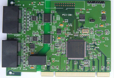
5. Bare boards (no parts on top) are often called "Printed Wiring Board (PWB)". The base plate of the board itself is made of materials that are insulated and heat-insulated, and not easy to bend. The small circuit material that can be seen on the surface is copper foil. The copper foil was originally covered on the entire board, but part of it was etched away during the manufacturing process, and the remaining part became a network of small lines. . These lines are called conductor patterns or wiring, and are used to provide circuit connections for parts on the PCB.
6. In the PCB design process, the color of the PCB board is usually green or brown, which is the color of the solder mask. It is an insulating protective layer that can protect the copper wire, prevent short circuits caused by wave soldering, and save the amount of solder. A layer of silk screen is also printed on the solder mask. Usually words and symbols (mostly white) are printed on this to mark the position of each part on the board. The screen printing surface is also called the legend surface.
When the final product is made, integrated circuits, transistors, diodes, passive components (such as resistors, capacitors, connectors, etc.) and various other electronic parts will be installed on it. Through the wire connection, the electronic signal connection can be formed and the application function can be formed.