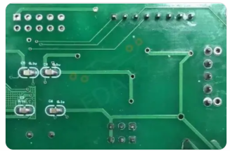
High-speed PCB design analysis: how to check the analog and signal integrity?
Put the printed circuit board together with high-speed signals, including design, components, and juggling of high-speed signals. These high-speed signals create opportunities for unnecessary transmission lines, causing serious damage to the circuit board. Most of the confusion occurs within the PCB layout itself.
Understanding the damage caused by the layout can achieve resolution when laying the circuit board. Understand whether the layout technology you are applying is the best practice for signal integrity analysis in PCB design. It can be discovered by performing lengthy pencil analysis or using signal integrity simulation tools. After reading, I will let you decide what you think is more effective for your circuit board.
1. Insufficient signal integrity simulation tools
With signal integrity simulation tools, the magic becomes confusing. The impedance calculator returned an incorrect impedance calculation. The calculation contradicts the material stacking and dielectric constant defined in the PCB design rules. The simulator assumes the modeled return path, so if there are discontinuities in the ground plane, they are not included in the calculation. The 3D field solver returns the calculated impedance of the differential pair that is very wrong.

The tool is very simple, does not support the general options of PCB layout, while keeping the design rules in mind. This includes rules and simulations of rigid bending. Its simulation environment produces incomprehensible waveforms. Further research requires complex manual commands to evaluate common operations. The same is true for its 3D field solver. Since the user interface has no option to analyze long electrical traces, there is no confidence in the layout of the circuit board to achieve high-speed signal integrity.
2. Interpretation of the time interval of the results
Spend hours to analyze the simulation tool results to analyze the dazzling errors. Navigating the menu requires meticulous work. Time sinks through the impedance calculator, revealing the use of incorrect parameters to calculate the trace impedance. Take the time to discover that the parameters used by the simulator do not match the net rules of the PCB layout. Who would guess?
If the inherent capacitance and dielectric constant of the planar material do not have the correct parameters, the calculated impedance will indeed reduce the reflection and ringing of high-speed signals.
Hidden environment anomalies (such as missing drill files) will cause the simulator to fail. Given the large number of PCB editors and settings required to set up the simulation, missing drill files can cause errors and cause confusion in the setup process. It will cause a challenge and re-inquiry on the parameters selected in the editor and the settings menu.
Searching through help pages and application descriptions can lead to more time wasted when analyzing tools that simulate high-speed signals to ensure signal integrity. Finally, the waveform obtained to illustrate the simulation results often shows garbage. It is frustrating if there is no elegant user interface to use powerful tools at my fingertips to correctly drive them to my circuit board. At the end of the day, integrity can still be contested.
3. Qualified tools to identify and resolve integrity
Wouldn't it be great if the impedance calculator in the tool used the material parameters set in the PCB design rules? Storing tool port information in its overall design rules to calculate impedance ensures that the printed circuit board will be returned from the manufacturer and supplement the circuit design with the correct components and layout.
Use the simulator to use the parameters to gain confidence in the results from the PCB design rules. In those days when engineers and layout designers solved signal integrity problems and solutions, obtaining the simulation results of waveforms displayed during schematic capture and PCB layout will help constructively improve the design. It eliminates the guesswork of performing analysis and applies best practices from pencil meditation, waiting for PCB manufacturing, and then verifying signal integrity.
Use precise waveform analysis
There is an impedance formula editor in the PCB layer stack manager. The layer stack manager can be easily accessed in the PCB layout environment through the drop-down menu. The impedance formula editor contains the correct routing impedance formulas for all topologies, including embedded, dual-link and differential network microstrip to stripline. The default formula for each topology can be easily accessed in the editor. This allows direct access to the formulas of each topology for easy modification in the tool. As an alternative, if it is more convenient, you can also access and edit the impedance formula through the query assistant.
4. Easily access the impedance formula editor through the layer stack manager
Once the impedance of reflections and ringing has been incorporated into the PCB layout, the signal integrity simulator can be set to analyze high-speed signal behavior. The simulator accepts the signal stimulus defined by the designer. The PCB designer also includes the parameter characteristics of high-speed signal networks, such as overshoot and undershoot values, flight time, and power network limitations.
The simulator uses these values to display the results in the waveform analysis window. The resulting waveforms show signal integrity issues, such as ringing, reflections, crosstalk, or voltage drops on high-speed lines due to PCB layout or filter discrete characteristics. PCB designers can adjust the impedance to achieve maximum signal integrity and continue to perform waveform analysis until the design is noise-free.