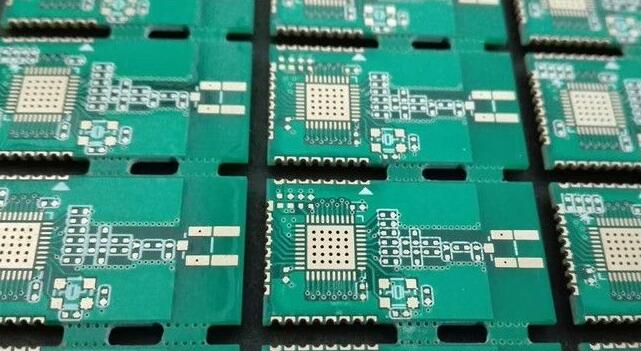
In the PCB industry, a printed circuit board (PCB) with a copper foil thickness equal to or greater than 105 μm (≥3 oz) is called a thick copper printed circuit board. The application field and demand for thick copper PCB have been rapidly expanded in recent years, and it has become a popular PCB variety with good market development prospects. The vast majority of thick copper printed circuit boards are high-current substrates, and high-current substrates are mainly used in two areas: power modules (power modules) and automotive electronic components. The development trend of this kind of high-current substrate is to carry a larger current, and the heat from a larger device needs to be dissipated, and the thickness of the copper foil used for the substrate is getting thicker. For example, the use of 210 μm thick copper foil for high-current substrates has become commonplace; another example is to replace the original busbars and wiring harnesses used in automobiles, robots, and power supplies. The thickness of the conductor layer of the substrate has reached 400 μm. ~2000 μm.
105 μm thick copper printed circuit boards have difficulties in solder mask production. Due to the limitation of the thickness of the ink on the substrate (the navigation mark has requirements for the thickness of the ink on the substrate and the thickness of the ink on the substrate is too thick,

it will cause the problem of solder resist cracks in the substrate position after the printed circuit board is welded) electrostatic spraying or spraying technology cannot be used Production. At present, the two processes in the industry can only use traditional screen printing: one is to print multiple solder masks, and the other is to make the substrate first, fill the substrate with the solder mask and then treat it as a normal PCB for normal printing solder mask., But screen printing will have quality problems such as solder mask entry holes, broken solder mask bridges, and air bubbles between lines. How to realize it can be produced by electrostatic spraying or spraying process. And can ensure that the thickness of the solder mask at the position of the base material is not too thick? This is the purpose of our research.
1 Method implementation
1.1 Planning stage
(1) Planning the direction. The method provided is to change the design engineering data to make solder mask exposure film to achieve. After the previous multiple solder masks, the ink on the substrate position is developed and the ink on the edge of the line is retained. The last time is regarded as a normal PCB production, so that there is only one solder mask on the substrate, and there is no problem of redness of the circuit.
(2) Planning process. Pre-treatment of solder mask - plug hole - electrostatic spraying - registration exposure (special design film) - development - post solder mask baking - pre-treatment of solder mask - plug hole - electrostatic spraying - registration exposure 1 (normal film) - development - resist Bake after welding 1……
2.2 Test phase
(1) Multiple solder mask production in the front. Use electrostatic spraying or spraying technology to produce (avoid soldering into the hole during spraying), and use specially designed solder mask exposure film materials for solder mask exposure.
(2) The last solder mask production. Use electrostatic spraying or spraying process to produce (avoid soldering into the hole during spraying), use normal solder mask to expose the negative film material during solder mask exposure, and the effect after solder mask is completed
(3) Substrate position ink thickness slice
2.3 Standardized promotion stage
Using the data and process developed by this process design, the production board is tested in small and medium batches, and the batch test results are consistent with the test results in the initial stage of the test. For all copper printed circuit boards with a thickness of 105 mm or more, if this process is used in the solder mask production, the product quality can be greatly improved.
3 results
The development of the above new processes, on the one hand, can normally use electrostatic spraying or spraying processes to solve the problem of solder mask production of copper printed circuit boards with a thickness of 105 mm or more, which cannot be solved by traditional screen printing. At the same time, it can avoid the problem of solder mask cracks when the ink is too thick at the base material position of the solder mask. It can smoothly mass-produce solder masks for copper printed circuit boards with a thickness of 105 mm and satisfy customers at the same time. Quality requirements for solder mask.
After using the above PCB manufacturing process, the bottleneck of the smooth mass production of copper printed circuit boards with thickness of 105 mm or more has been solved, and the scrap rate has been reduced from 1.2% to 0.3%, making the copper printed circuit boards with thickness of 105 mm or more used in power supplies. Products, as well as communications, power, aerospace and other fields are guaranteed.