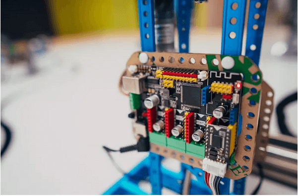
The PCB copy board is also the circuit board copy board. There are about ten steps, which will be explained one by one below.
Ten steps of PCB copy board:
1. Get a piece of PCB, first record the model, parameters, and positions of all vital parts on paper, especially the direction of the diode, the direction of the three-machine tube, and the direction of the IC gap. It is best to use a scanner to scan two photos of the location of vital parts, which will be of great help to restore the prototype in the future.
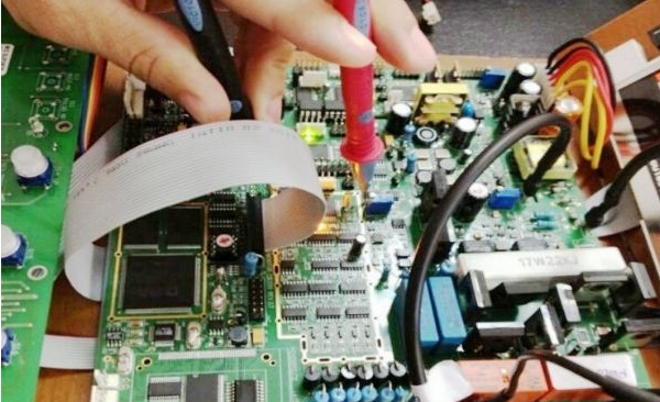
2. Remove all components and remove the tin in the PAD hole. Rinse the empty PCB board with ultrasound, and then put it into the scanner. Note that the PCB must be placed horizontally and straight in the scanner, otherwise the scanned image will be unusable. Then open the Photoshop software and input it into the scanner. Set the scan DPI "resolution" at this time after startup, which can be set according to different densities, if the setting is 600DPI. Scan the silk screen surface in color and save the name to customize it. The bottom silk screen method is the same.

3. Lightly polish the two layers of TOP LAYER and BOTTOM LAYER with water gauze paper until the copper film is shiny, put them into the scanner, start the PHOTOSHOP software, scan the two layers in color and save them separately. "Attention" The PCB must be placed horizontally and straight in the scanner.
4. Adjust the size, contrast, and brightness of the canvas to make the part with copper film and the part without copper film have a strong contrast, then turn the second image into black and white, check whether the lines are clear, if not, repeat this step. If it is clear, save the picture as black and white BMP format files TOP.BMP and BOT.BMP.
Five, will BOT. BMP is converted to BOT. PCB, pay attention to the conversion to the SILK layer, which is the light yellow layer, and then you can trace on the BOT layer. Delete the SILK layer after drawing.
6. Convert TOP.BMP to TOP.PCB, pay attention to the conversion to the SILK layer, which is the yellow layer, and then you can trace the line on the TOP layer, and place the device according to the drawing in the second step. Delete the SILK layer after drawing.
7. Convert the two BMP format files to PROTEL format files, and transfer to two layers in PROTEL. For example, the positions of PAD and VIA after two layers basically coincide, indicating that the previous steps are well done. If there is a deviation, Then repeat the fourth step of the third step.
8. TOP in PROTEL. PCB and BOT. Import the PCB and combine it into one picture and it's OK.
9. The copying process of the same middle layer is also the same. Repeat steps 5 and 6, and the final output PCB file is the same PCB diagram as the actual product.
The difficulty of PCB copy board operation is mainly related to the number of sub-layers and device density of the two-point board above, as well as other aspects, such as the integrity of the board.
10. Compare the original picture with the PCB copy board, that is, the 1:1 file after copying the circuit board. If it's correct, you're done.