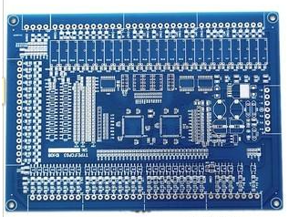
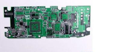
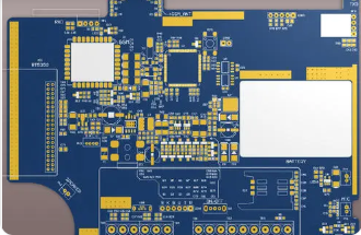
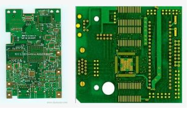
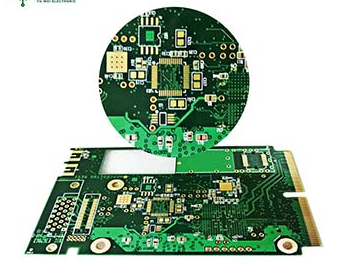
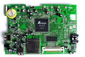
PCBA processing manufacturers PCBA chip processing and production process, due to the influence of operating errors, it is easy to cause PCBA patch defects, such as: air welding, short circuit, erection, missing parts, tin beads, squatting feet, floating height, wrong parts, cold welding, Reverse, reverse white/reverse, offset printing, component damage, low tin, poly tin, gold finger tin, overflow glue, etc., these defects need to be analyzed, improved, and product quality improved.
Analysis of Causes of PCBA Chip Processing Defects
First, air welding
1. The activity of solder paste is weak;
2. The steel mesh opening is not good;
3. The copper or platinum spacing is too large or large copper paste small components;
4. The blade pressure is too large;
5. The component feet are not flat (warped, deformed);
6, the reheating zone of the reflow furnace is heating up too fast;
7, PCB coppe r platinum is too dirty or oxidized;
8, PCB board contains water;
9. Machine placement offset;
10. Solder paste printing offset printing;
11.The looseness of the machine plywood guide rail causes the placement to shift;
12. The misalignment of the MARK point due to the misalignment of the components causes the welding to be empty;
Second, short circuit

1. The distance between the steel mesh and the PCB is too large, which causes the solder paste to be printed too thick and short;
2. The component placement height is set too low to squeeze the solder paste and cause a short circuit;
3. The heating furnace heats up too fast;
4. Caused by component placement offset;
5. The stencil opening is not good (the thickness is too thick, the lead opening is too long, and the opening is too large);
6, the solder paste cannot bear the weight of the component;
7, the deformation of the stencil or squeegee causes the solder paste to be printed too thick;
8. Strong solder paste activity;
9, the empty paste point sealing tape is rolled up, causing the solder paste of the peripheral components to be printed too thick;
10. The reflux vibration is too large or not level;
Third, stand upright
1, Copper and platinum on both sides of different sizes produce uneven tension;
2. The preheating speed is too fast;
3. Machine placement offset;
4. The printing thickness of solder paste is uneven;
5. The temperature distribution in the reflow furnace is uneven;
6. Solder paste printing offset printing;
7, the machine track splint is not tight, resulting in an offset;
8, the machine head shakes;
9, the activity of the solder paste is too strong;
10.The furnace temperature is not set correctly;
11.The distance between copper and platinum is too large;
12. Yuan song caused by incorrect operation of MARK point
Fourth, missing parts
1. The carbon sheet of the vacuum pump has insufficient vacuum, resulting in missing parts;
2. The nozzle is clogged or the nozzle is defective;
3. Improper detection of component thickness or poor detector;
4. Improper placement height;
5. The nozzle is too big or does not blow;
6.Improper nozzle vacuum setting (applicable to MPA);
7. The placement speed of special-shaped components is too fast;
8. The head of the trachea is very fierce;
9, the valve seal is worn;
There are foreign objects on the side of the reflow oven track to wipe the components on the board;
Fifth, tin beads
1. Insufficient preheating of reflow soldering and too fast heating;
2. The solder paste is refrigerated and the temperature is not complete;
3. The solder paste absorbs splashes (the indoor humidity is too heavy);
4. There is too much water on the PCB board;
5. Add excess diluent;
6.Improper design of the steel mesh opening; 7.The tin powder particles are not uniform.
Sixth, offset
1. The positioning reference point on the board is not clear
2.The positioning reference point on the circuit board is not aligned with the reference point of the template.
3. The fixed clamping of the circuit board in the printing machine is loose. The positioning thimble is not in place.
4. The optical positioning system of the printing press is faulty
5. The solder paste lacks the template opening and does not match the circuit board design file
In order to improve the defects of the PCBA patch, it is necessary to conduct strict inspections on all aspects to prevent the problems of the previous process from flowing into the next process as little as possible.