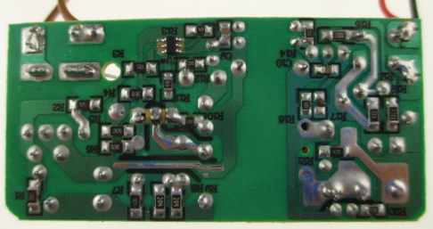
For electronic product designers, especially circuit board designers, product design for manufacturability (DFM) is a factor that must be considered. If the circuit board design does not meet the design requirements for manufacturability, it will greatly Reduce the production efficiency of the product, and in severe cases may even cause the designed product to be unable to be manufactured at all. At present, Through Hole Technology (THT) is still in use. DFM can play a great role in improving the efficiency and reliability of through hole manufacturing. DFM method can help through hole manufacturing. The supplier reduces defects and maintains competitiveness.
1. Typesetting and layout
Proper layout in the design stage can avoid a lot of troubles in the manufacturing process.
(1) Using a large board can save materials, but due to warpage and weight, it will be difficult to transport in production. It needs to be fixed with special fixtures, so avoid using a board larger than 23cm*30cm. It is best to control the size of all boards within two or three types, which helps to reduce the downtime caused by adjusting the guide rail and repositioning the position of the bar code reader when the product is replaced. Also, it is possible to have fewer board sizes. Reduce the number of wave soldering temperature curves.
(2) It is a good design method to include different kinds of jigsaw boards in a board, but only those boards that are finally built into a product and have the same production process requirements can be designed in this way.
(3) Some frames should be provided around the board, especially when there are components on the edge of the board, most automatic assembly equipment requires at least a 5mm area on the board edge.

(4) Try to make wiring on the top surface (component surface) of the board, and the bottom surface (welding surface) of the circuit board is easy to be damaged. Do not route wires close to the edge of the board, because the edges of the board are used for grasping during the production process, and the lines on the edge will be damaged by the claws of the wave soldering equipment or the frame conveyor.
(5) For devices with a large number of pins (such as terminal blocks or flat cables), oval pads should be used instead of circular to prevent solder bridges during wave soldering (Figure 1).
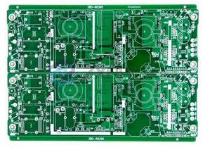
Manufacturability Design of Through Hole PCB
(6) Make the positioning hole spacing and the distance between it and the component as large as possible, and standardize and optimize its size according to the insertion equipment; do not electroplate the positioning hole, because the diameter of the plating hole is difficult to control.
(7) Try to make the positioning hole also be used as the mounting hole of the PCB in the final product, so as to reduce the drilling process during production.
2. Positioning and placement of PCB components
(1) Arrange the components in rows and columns according to a grid pattern position. All axial components should be parallel to each other, so that the axial inserting machine does not need to rotate the PCB when inserting, because unnecessary rotation and movement will greatly Reduce the speed of the inserting machine. The components placed at a 45-degree angle like Figure 2 cannot actually be inserted by the machine.
(2) Similar components should be arranged in the same way on the board. For example, make the negative poles of all radial capacitors face the right side of the board, make the notch marks of all dual in-line packages (DIP) face the same direction, etc., which can speed up the insertion speed and make it easier to find errors. As shown in Figure 3, because the A board uses this method, it is easy to find the reverse capacitor, while the B board search takes more time. In fact, a company can standardize the direction of all circuit board components it manufactures. Some board layouts may not necessarily allow this, but this should be a direction of effort.
(3) The arrangement direction of dual in-line package devices, connectors and other multi-pin count components is perpendicular to the direction of wave soldering, which can reduce the tin bridge between component pins.
(4) Make full use of the silk screen to mark the board surface, for example, draw a frame for bar code, print an arrow to indicate the direction of wave soldering on the board, and use the dotted line to trace the outline of the bottom surface component (so that the board only needs to be screen printed once. )and many more.
(5) Draw the component reference symbol (CRD) and polarity indication, and they will still be visible after the component is inserted. This is very helpful in checking and troubleshooting, and it is also a good maintenance job.
3. Machine plug-in
(1) The pads of all the components on the board should be standard, and the industry standard separation distance should be used.
(2) The selected components should be suitable for machine insertion. Keep in mind the conditions and specifications of the equipment in your own factory, and consider the packaging form of the components in advance to better cooperate with the machine. For special-shaped components, packaging may be a bigger problem.
(3) If possible, use the axial type as far as possible for the radial element, because the insertion cost of the axial element is relatively low. If the space is very precious, the radial element can also be used first.
4. Wires and connectors
(1) Do not connect wires or cables directly to the PCB, but use connectors. If the wire must be soldered directly to the board, the end of the wire must be terminated with a wire to the board's terminal. The wires connected from the circuit board should be concentrated in a certain area of the board, so that they can be sheathed together to avoid affecting other components.
(2) Use wires of different colors to prevent errors in the assembly process. Each company can use its own set of color schemes, for example, the high bits of all product data lines are represented by blue, and the low bits are represented by yellow.
(3) Connectors should have larger pads to provide better mechanical connections, and the leads of high-pin-count connectors should be chamfered for easier insertion.
5. The whole system
(1) The components should be selected before designing the printed circuit board, so that the best layout can be achieved and will help implement the DFM principles described in this article.
(2) Avoid using some parts that require machine pressure, such as wire pins, rivets, etc. In addition to the slow installation speed, these parts may also damage the circuit board, and their maintainability is also poor.
(3) Use the following method to minimize the types of components used on the board: replace a single resistor with a row resistor; replace two three-pin connectors with a six-pin connector; if the values of the two components are very similar, but the tolerances are different, Then use the one with the lower tolerance for both positions; use the same screws to fix the various heat sinks on the board.
6. Routine requirements
(1) When conformal coating is applied to the circuit board, the parts that do not need to be coated should be marked on the drawing during the engineering design. The influence of the coating on the capacitance between lines should be considered in the design.
(2) For through holes, in order to ensure the best welding effect, the gap between the pin and the aperture should be between 0.25mm and 0.70mm. A larger pore size is beneficial for machine insertion, and a smaller pore size is required to get a good capillary effect, so a balance between the two needs to be struck.
(3) Components that have been preprocessed according to PCB industry standards should be selected. Component preparation is one of the least efficient parts of the production process. In addition to adding additional processes (corresponding to the risk of electrostatic damage and prolonging the delivery time), it also increases the chance of error.
7. Conclusion
For PCB manufacturers who use through-hole plug-in technology for circuit board assembly, DFM is an extremely useful tool, which can save a lot of money and reduce a lot of trouble. Using the DFM method can reduce engineering changes and make concessions on the design in the future, these benefits are very direct.