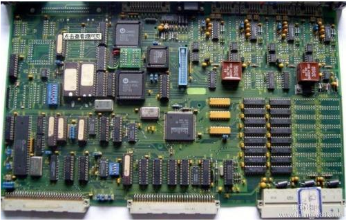
Laser marking is a very advanced marking technology. Through the focused laser engraving technology, the characters and patterns that need to be marked are engraved on the surface of the object. Compared with traditional printing technology, laser marking has the characteristics of good quality, high consistency, strong wear resistance, high efficiency, cost saving, safety and reliability, etc., and it is widely used in the circuit board (PCB) industry.
Market demand under technological progress
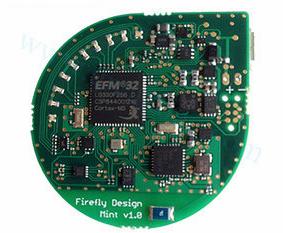
With the rapid development of the IT industry, smart phones, wearable electronics and other products continue to develop towards lightness, thinness and miniaturization. Consumers have higher and higher requirements for electronic products, and the production of PCB boards must also be improved. In order to achieve the quality control of the PCB production process, marking characters, one-dimensional codes, two-dimensional codes and other information on the PCB for traceability has become the development trend of the industry.
Traditional printing technology is increasingly unable to adapt to the new market technology needs due to problems such as poor wear resistance, low precision, poor aesthetics, and environmental pollution. Therefore, laser marking has become a trend in the PCB industry.

The defects of traditional printing technology
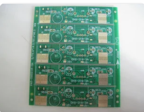
Marking on the surface of the PCB board like pattern drawing, company LOGO printing, contact information, two-dimensional code, etc., in the past, silk screen printing in traditional printing was usually used. Under the original market demand, traditional printing technology can also meet the requirements of the market. However, as the quality of electronic products continues to improve, consumers' requirements are getting higher and higher, resulting in higher and higher marking quality of PCB boards in the market. Traditional printing Technology cannot adapt to new market requirements, and its shortcomings are becoming more and more obvious.
1. Poor abrasion resistance. The abrasion resistance mentioned here is not the abrasion resistance of metal materials. It refers to the situation that the ink on the surface of the circuit board is often worn away during use, resulting in blurring, discoloration, etc.
2. Aesthetic requirements, the appearance of metal surface printing is relatively low-end, which is not suitable for some products with high appearance requirements, such as medals, metal business cards, exquisite company publicity nameplates, handicraft description nameplates, etc. Meet its appearance requirements.
3. In the ordinary printing process, organic solvents and heavy metal elements and other chemical raw materials are needed. These substances are toxic and can cause personal injury to the screen printing staff. In addition, during the drying process of the screen printing ink, the volatile chemical raw materials gradually volatilize into the air., Pollution to the air and the environment.
Unique advantages of laser marking
The emergence of laser marking technology has successfully solved a series of problems in traditional printing technology. It is characterized by high marking accuracy, fast speed and stable performance. Moreover, it only needs to be controlled by a computer, and the operation is simple, and it can print various complicated patterns, characters, two-dimensional codes and other content, which fully meets the high-quality marking requirements of the existing circuit board industry.
Compared with traditional printing technology, laser marking technology has many advantages:
1. Good quality and strong wear resistance. The marking on the surface of the PCB board is clear and beautiful, and various LOGO, patterns, two-dimensional codes, and text can be marked, and the patterns are directly engraved on the material, which has more outstanding abrasion resistance;
2. High processing precision. After the laser beam emitted by the laser is focused, the minimum spot diameter can reach 10um (UV laser), which is of great help when dealing with complex graphics and precision processing;
3. High efficiency, simple operation and lower cost. The user only needs to set the parameters on the computer to mark directly, and the surface marking of the material can be completed in just a few seconds to ten seconds.
4. Non-destructive marking. Laser marking uses non-contact processing, the laser head does not need to touch the surface of the material, so there is no need to consider the damage to the material;
5. Wide range of use, safety and environmental protection. All kinds of thin metal/non-metal materials can be marked;
6. Stable performance and long service life of the equipment. With the development of technology, the service life of lasers has been greatly increased, and the service life of equipment has been greatly lengthened.
Application of UV laser marking and CO2 laser marking technology in PCB industry
In the laser marking application of PCB boards, UV laser marking and CO2 laser marking are the most used. UV laser marking and CO2 laser marking have become the preferred technology for PCB surface marking due to their low thermal impact, good processing effect, high precision, and high speed.
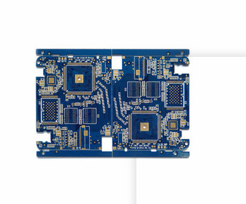
The use of laser marking two-dimensional code technology in the PCB industry can realize PCB production, process, and quality traceability, and realize automated and intelligent management requirements to meet the needs of lean production, quality control, and process improvement. Marking two-dimensional codes on the PCB surface is currently a common demand of mid- to high-end customers and has been widely used.