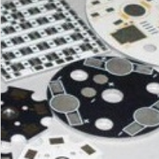
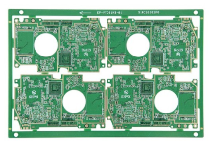
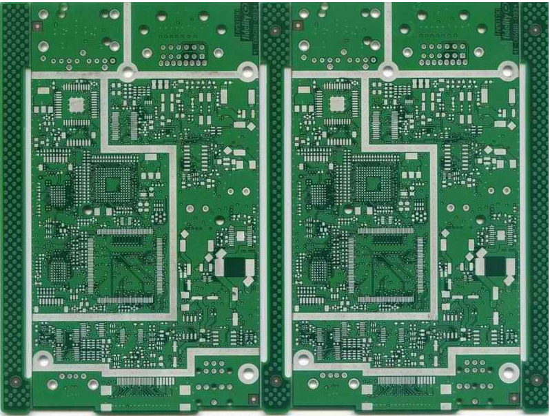
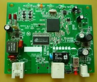
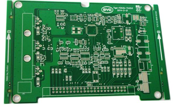
With the rapid development of the electronics industry, PCB wiring is becoming more and more sophisticated. Most PCB manufacturers use dry film to complete graphics transfer, and the use of dry film is becoming more and more popular. However, I still encounter many problems in the after-sales service process. Customers have a lot of misunderstandings when using dry film, which are summarized here for reference.
1. There are holes in the dry film mask
Many customers believe that after a hole occurs, the film temperature and pressure should be increased to enhance its bonding force. In fact, this view is incorrect, because the solvent of the resist layer will evaporate excessively after the temperature and pressure are too high, which will cause dryness. The film becomes brittle and thinner, and the holes are easily broken during development. We must always maintain the toughness of the dry film. Therefore, after the holes appear, we can make improvements from the following points:
1, reduce the temperature and pressure of the film

2, to improve drilling and piercing
3, increase the exposure energy
4, reduce developing pressure
5, the parking time after the film is not too long, so as not to cause the semi-fluid film in the corner to spread and thin under the action of pressure
6, do not stretch the dry film too tightly during the pasting process
Second, seepage plating occurs during dry film electroplating
The reason for the permeation is that the dry film and the copper clad board are not firmly bonded, which causes the plating solution to deepen, which causes the "negative phase" part of the coating to become thicker. The permeation of most PCB manufacturers is caused by the following points:
1, the exposure energy is high or low
Under ultraviolet light irradiation, the photoinitiator that has absorbed the light energy decomposes into free radicals to initiate a photopolymerization reaction to form a body-shaped molecule that is insoluble in a dilute alkali solution. When the exposure is insufficient, due to incomplete polymerization, the film swells and becomes soft during the development process, resulting in unclear lines or even the film layer falling off, resulting in poor bonding between the film and copper; if the exposure is overexposed, it will cause development difficulties and also during the electroplating process. Warping and peeling occurred during the process, forming penetration plating. Therefore, it is very important to control the exposure energy.
2, the film temperature is high or low
If the film temperature is too low, the resist film cannot be sufficiently softened and flowed properly, resulting in poor adhesion between the dry film and the surface of the copper clad laminate; if the temperature is too high, the solvent and other volatility in the resist The rapid volatilization of the substance produces bubbles, and the dry film becomes brittle, causing warping and peeling during electroplating electric shock, resulting in infiltration.
3, the film pressure is too high or low
When the film pressure is too low, it may cause uneven film surface or gaps between the dry film and the copper plate and fail to meet the requirements of the bonding force; if the film pressure is too high, the solvent and volatile components of the resist layer will volatilize too much, causing The dry PCB film becomes brittle and will be lifted and peeled after electroplating electric shock.