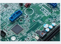
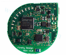
PCB modification refers to the rectification and design of the original product design and circuit board layout and wiring design on the premise of maintaining the same original function, adjusting the layout of the components on the board and the direction of the circuit, and realizing the redesign and development of electronic products. At the same time, it can avoid intellectual property rights and other disputes, accelerate the development of new products, and follow up with the latest development trends in PCB technology. PCB modification is just like PCB design. PCB files need to be modified. In this process, we need to pay attention to many details like PCB design. What should we pay attention to when PCB modification? (In the process of making PCB copy board, you should also pay attention to the following points to pay attention to)
As an electronic engineer designing a PCB circuit is a necessary hard work, but no matter how perfect the principle design is, if the PCB circuit board design is unreasonable, the performance will be greatly reduced, and it may even not work properly in severe cases. Based on my experience, I have summarized the following points that should be paid attention to in PCB modification, and I hope it can be enlightened to you.
No matter what software is used, there is a general procedure for PCB modification, which will save time and effort in order, so I will introduce it according to the production process.
1. The PCB schematic design is the preliminary work. It is often seen that beginners directly draw PCB boards in order to save trouble. This will outweigh the gains. For simple PCB boards, if you are proficient in the process, you can skip it. But for beginners, you must follow the process, so that on the one hand, you can develop good habits, and on the other hand, the only way to avoid mistakes for complex PCB circuits.

When drawing the PCB schematic diagram, pay attention to the various files to be connected as a whole in the hierarchical design. It is best to draw it according to each functional module, so that it will appear that your PCB schematic diagram is also important for future work. Due to differences in software, some software may appear to be connected but not connected (in terms of electrical performance). If you don’t use related testing tools, in case something goes wrong, it’s too late to find out when the board is ready. Therefore, the importance of doing things in order has been repeatedly emphasized, and I hope to attract everyone's attention.
2. The PCB schematic diagram is based on the designed project, as long as the electrical connection is correct, there is nothing to say. Below we focus on the problems in the specific board-making procedures.
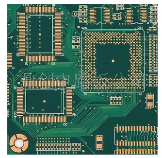
l. Make a physical frame
The closed physical frame is a basic platform for the future component layout and routing, and it also plays a constraining role for the automatic layout. Otherwise, the components coming from the schematic will be at a loss. But you must pay attention to accuracy here, otherwise installation problems in the future may be troublesome. In addition, it is best to use arcs at the corners. On the one hand, it can avoid sharp corners from scratching workers, and at the same time, it can reduce the effect of stress. In the past, one of my products always had the PCB board of the face shell broken during the transportation process, and it was just fine after using the arc.
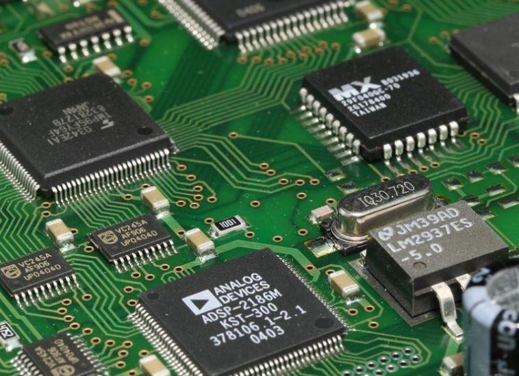
2. The introduction of components and networks
It should be very simple to draw the components and the network in the good frame, but there are often problems here. You must carefully solve the errors one by one according to the prompts. Otherwise, it will take more effort. The problems here are generally as follows:
The package form of the component can not be found, the component network problem, there are unused components or pins, these problems can be solved quickly by comparison.
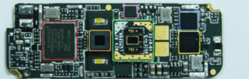
3. Layout of components
The layout and wiring of the components have a great impact on the life, stability, and electromagnetic compatibility of the product, so special attention should be paid. Generally speaking, there should be the following principles:
1) Placement order
First place the components related to the structure at a fixed position, such as power sockets, indicator lights, switches, connectors, etc. After these components are placed, use the lock function of the software to lock them so that they will not be moved by mistake in the future. Then place special components and large components on the circuit, such as heating components, transformers, ICs, etc. Finally, place the small device.
2) Pay attention to heat dissipation
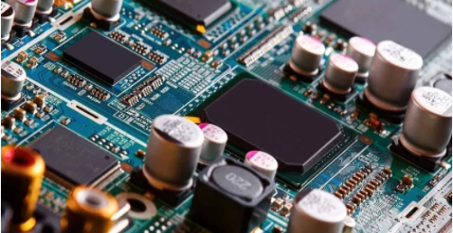
Particular attention should be paid to heat dissipation in the component layout. For high-power circuits, the heating elements such as power tubes, transformers, etc. should be placed as close to the side as possible to facilitate heat dissipation. Do not concentrate in one place, and do not have high capacitors too close to avoid premature aging of the electrolyte.
4. Wiring
Wiring principle
◆High-frequency digital circuit traces should be thinner and shorter
◆Attention should be paid to isolation between high current signal, high voltage signal and small signal (the isolation distance is related to the withstand voltage to be withstood. Normally, the distance between the board should be 2mm at 2KV, and it should be increased in proportion to this. For example, to withstand the 3KV withstand voltage test, the distance between the high and low voltage lines should be more than 3.5mm. In many cases, to avoid creepage, slots are also slotted between the high and low voltages on the printed circuit board.)
◆When wiring two panels, the wires on both sides should be perpendicular, oblique, or bent to avoid parallel to each other to reduce parasitic coupling; printed wires used as the input and output of the circuit should be avoided as far as possible. In order to avoid feedback, it is best to add a grounding wire between these wires.
◆The corners of the routing should be as large as possible to be greater than 90 degrees, to eliminate corners below 90 degrees, and to minimize the use of 90 degrees corners.
◆The same address line or data line, the length of the trace should not be too different, otherwise the short line part must be artificially bent for compensation
◆The trace should be on the soldering surface as much as possible, especially the PCB of the through-hole process
◆Use as few vias and jumpers as possible
◆Single-panel pads must be large, and the wire connecting the pads must be thick, and teardrops can be placed when teardrops can be placed. The quality of general single-panel manufacturers will not be very good, otherwise there will be problems with soldering and RE-WORK.
◆Large area copper should be covered with a grid to prevent bubbles and bending of the board due to thermal stress during wave soldering. However, in special occasions, the flow direction and size of the GND should be considered. You cannot simply fill it with copper foil., But need to route
◆The components and traces should not be placed too close to the side. The general single-sided boards are mostly paper boards, which are easy to break after being stressed. If they are connected or placed on the edge, they will be affected.
◆Convenience of production, debugging and maintenance must be considered
3. It is very important for analog circuits to deal with the ground problem. The noise generated on the ground is often inconvenient to predict, but once it is generated, it will bring great troubles. For the power amplifier circuit, the extremely small ground noise will have a significant impact on the sound quality due to the amplification of the subsequent stage; in the high-precision A/D conversion circuit, if there is a high-frequency component on the ground wire, a certain temperature drift will occur. The work of the amplifier. At this time, decoupling capacitors can be added to the 4 corners of the board, one foot is connected to the ground on the board, and the other foot is connected to the mounting hole (connected to the case by screws), so that this component can be taken into account. The amplifier and AD are also It's stable.
To do a good job of PCB modification, it is not just imitating PCB copy board. This is why so many companies in the industry fail when making PCB modification for customers, because they never care about so many problems., I think there is only a PCB file for the customer.