PCB copy board, that is, under the premise that there are already physical objects of electronic products and circuit boards, reverse analysis of the circuit boards by reverse research and development technology, and the original product PCB files, bill of materials (BOM) files, and schematic files Perform a 1:1 restoration of technical documents and PCB silk screen production documents, and then use these technical documents and production documents to perform PCB manufacturing, component welding, flying probe testing, circuit board debugging, and complete the complete copy of the original circuit board template.
Since electronic products are composed of various types of circuit boards, the core control part performs work. Therefore, the use of a process of PCB copying can complete the extraction of a full set of technical data of any electronic product and the imitation and cloning of products.
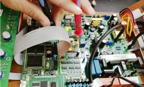
Let's show you the PCB copy board secret technique:
The first step is to get a PCB. First, record the model, parameters, and positions of all vital parts on the paper, especially the direction of the diode, the three-machine tube, and the direction of the IC gap. It is best to use a digital camera to take two photos of the location of the vital parts.

The second step is to remove all the components and remove the tin in the PAD hole. Clean the PCB with alcohol, then put it in the scanner, start POHTOSHOP, scan the silk screen surface in color, and print it out for later use.
The third step is to lightly polish the TOP LAYER and BOTTOM LAYER with water gauze paper until the copper film is shiny, put it in the scanner, start PHOTOSHOP, and scan the two layers in color separately. Note that the PCB must be placed horizontally and straight in the scanner, otherwise the scanned image cannot be used.
The fourth step is to adjust the contrast and brightness of the canvas to make the part with copper film and the part without copper film have a strong contrast, then turn the second image into black and white, and check whether the lines are clear. If not, repeat this step. If it is clear, save the picture as black and white BMP format files TOP.BMP and BOT.BMP.
The fifth step is to convert the two BMP format files into PROTEL format files, and transfer two layers in PROTEL. For example, the positions of PAD and VIA that have passed through the two layers basically coincide, indicating that the previous steps are well done. If If there is a deviation, repeat the third step.
Sixth, convert TOP.BMP to TOP.PCB. Pay attention to the conversion to the SILK layer, which is the yellow layer. Then you can trace the line on the TOP layer and place the device according to the drawing in the second step. Delete the SILK layer after drawing.
The seventh step is to convert BOT.BMP to BOT.PCB, pay attention to the conversion to the SILK layer, which is the yellow layer, and then you can trace on the BOT layer. Delete the SILK layer after drawing.
The eighth step is to import TOP.PCB and BOT.PCB in PROTEL and combine them into one picture and it is OK.
The ninth step, use a laser printer to print the TOP LAYER and BOTTOM LAYER on the transparent film (1:1 ratio), put the film on the PCB board, compare whether there is any error, if it is correct, you are done NS.