The concept of solder mask
The solder mask is the solder mask, which refers to the part to be painted on the printed circuit board. In fact, this solder mask uses a negative output, so after the shape of the solder mask is mapped to the board, the solder mask is not painted with green oil, but the copper skin is exposed.

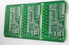
The printed circuit board is basically composed of pads, vias, solder mask, silk screen, copper wires, various components and other parts. Usually in order to increase the thickness of the copper skin, the solder mask is used to scribe lines to remove the green oil, and then tin is added to increase the thickness of the copper wire.
The role of solder mask
The basic structure of a printed circuit board is pads, vias, solder mask, and text printing. The solder mask is the yellow or red or black or green or other colors that you see. Some boards are yellow solder mask. The role of the solder mask is to prevent the parts that should not be soldered from being connected by solder. Reflow soldering is achieved by the solder mask. The hot tin water on the entire surface of the board, the exposed PCB board without the solder resist layer is wetted with tin, and the part with the solder resist layer is not wetted with tin.

Solder mask process requirements
Process requirements:
The role of the solder mask in controlling solder defects during the reflow soldering process is important, and the PCB designer should minimize the spacing or air gaps around the pad features.
Although many process engineers would rather separate all pad features on the board with the solder mask, the pin spacing and pad size of fine-pitch components will require special consideration. Although solder mask openings or windows that are not partitioned on the four sides of the qfp may be acceptable, it may be more difficult to control the solder bridges between the component pins. For the solder mask of bga.
Many companies provide a solder mask that does not touch the pads, but covers any features between the pads to prevent solder bridges. Most surface mount PCBs are covered with a solder mask, but if the thickness of the solder mask is greater than 0.04mm ("), it may affect the application of solder paste. Surface mount PCBs, especially those using fine pitch components, Both require a low-profile photosensitive solder mask.
Craft production:
Solder mask materials must be used through liquid wet process or dry film lamination. Dry film solder mask materials are supplied in a thickness of 0.07-0.1mm (0.03-0.04"), which can be suitable for some surface mount products, but this material is not recommended for close-pitch applications. Few companies provide thin enough to meet Fine pitch standard dry film, but there are several companies that can provide liquid photosensitive solder mask materials.
Generally, the solder mask opening should be 0.15mm (0.006") larger than the pad. This allows a gap of 0.07mm (0.003") on all sides of the pad. Low-profile liquid photosensitive solder mask materials are economical and are usually specified for surface mount applications, providing precise feature sizes and gaps.