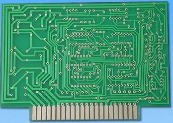
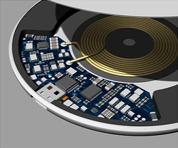
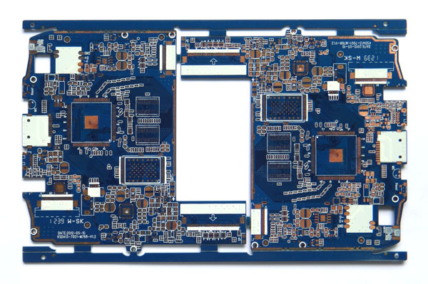
1. The PCB size and the number of wiring layers need to be determined at the early stage of the design
If the design requires the use of high-density ball grid array (BGA) components, the minimum number of wiring layers required for wiring these devices must be considered. The number of wiring layers and the stack-up method will directly affect the wiring and impedance of the printed lines. The size of the board helps determine the stacking method and the width of the printed line to achieve the desired design effect.
For many years, people have always believed that the lower the number of PCB layers, the lower the cost, but there are many other factors that affect the manufacturing cost of the PCB. In recent years, the cost difference between multilayer boards has been greatly reduced. It is best to use more circuit layers and evenly distribute the copper at the beginning of the design, so as to avoid discovering that a small number of signals do not meet the defined rules and space requirements until the end of the design, so that new layers are forced to be added. Careful planning before design will reduce a lot of trouble in wiring

2. The automatic wiring tool itself does not know what to do
In order to complete the wiring task, the wiring tool needs to work under the correct rules and restrictions. Different signal lines have different wiring requirements. All signal lines with special requirements must be classified, and different design classifications are different. Each signal class should have a priority, the higher the priority, the stricter the rules. The rules involve the width of the printed lines, the maximum number of vias, the degree of parallelism, the mutual influence between the signal lines, and the limitation of layers. These rules have a great influence on the performance of the wiring tool. Careful consideration of design requirements is an important step for successful wiring.
To optimize the assembly process, design for manufacturability (DFM) rules impose restrictions on component layout. If the assembly department allows the components to move, the circuit can be appropriately optimized, which is more convenient for automatic wiring. The defined rules and constraints will affect the layout design.
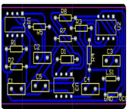
3. The routing channel and via area need to be considered during layout
These paths and areas are obvious to PCB designers, but the automatic routing tool only considers one signal at a time. By setting routing constraints and setting the layer of signal lines, the routing tool can be as the designer imagined Complete the wiring as shown.
In the fan-out design stage, in order to enable the automatic routing tool to connect the component pins, each pin of the surface mount device should have at least one via, so that when more connections are needed, the PCB can be internally layered Connection, online testing (ICT) and circuit reprocessing.
In order to maximize the efficiency of the automatic routing tool, the largest via size and printed line must be used as much as possible, and the interval is ideally set to 50mil. Use the via type that maximizes the number of routing paths. When carrying out fan-out design, it is necessary to consider the problem of circuit online testing. Test fixtures can be expensive, and they are usually ordered when they are about to go into full production. If only then consider adding nodes to achieve 100% testability, it would be too late.