It is worth noting that the reduction of PCB levels can greatly save costs. It can almost be said that the number of PCBs has doubled the cost of two layers. In other words, the cost of a four-layer PCB is twice that of two layers, and the cost of a six-layer PCB is twice that of four layers. The most luxurious EX58-EXTREME uses a 12-layer PCB, so it is also very expensive.
Using fewer PCBs plays a very important role in cost control. Most DIYers have not put the number of PCBs in the same important position as the GPU. In addition, PCB production is generally designed by chip manufacturers or more powerful manufacturers and handed over to PCB factories. The design of PCB determines how to walk and the placement of later components, which is also a very advanced technology.
For DIYer, how do we choose a complete material product. I believe that through our school article is very helpful to you. In any case, judging the number of PCB layers is a skill that must be mastered. Let us introduce some methods for judging the number of PCB layers.
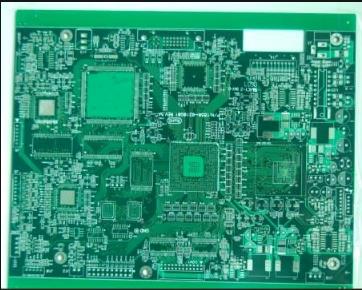
The first visual method. Due to the close integration of PCB layers, it is difficult to see the actual number, but if you carefully observe the defects of the board, you can still distinguish it. Carefully, we will find that there is one or more layers of white material in the middle of the PCB.

This is the insulation between the levels to ensure that there is no short circuit between the different PCB layers. Since the current multi-layer PCB board uses more single-sided or two-sided distribution boards, and an insulating layer is placed between each layer, this means that there are several independent distribution layers. The layer and the insulating layer between layers have become the most intuitive way to judge the number of PCB layers.
The second guide hole and blind hole alignment method. Via holes use the via holes on the PCB to identify the number of PCB layers.. The principle is mainly due to the multi-layer PCB circuit connection using via hole technology. We need to see how many layers of the PCB can be identified by observing the via holes.
In the most basic PCB (a mother board), the components are concentrated in one of them. If you want to use a multi-layer board, you need to pass through the board so that the guide holes of the component will pass through the PCB board. So we can see that some pins are soldered on the other side.
For example, the board uses a four-layer board, so it is necessary to move other layers, such as the ground layer and the power layer, on the first and fourth layers (signal layer). Placing the signal layer on both sides of the power layer and the ground layer can prevent mutual interference and easily correct the signal line. If some board guide holes appear on the front of the PCB but cannot be found on the other side, then it must be 6/8 layers. If the same guide holes can be found on the front and back of the PCB, it is a 4-layer board.
However, many card manufacturers use another method to connect some of these lines, and use buried vias and blind vias in the lines. Blind vias connect the PCB in several layers to the surface PCB without penetrating the entire circuit board.
The buried via is only connected to the internal PCB, so it is impossible to see only from the surface. Because the blind hole does not need to penetrate the entire PCB, if it is six layers or more, it will not pass through the light source. Therefore, there is also a very popular saying that PCBs with four layers and six layers or more are determined by whether the holes leak. This method has its reasons and inapplicability, which can be used as a reference method.
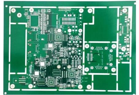
The third method of accumulation. To be precise, this is not a method, but an experience. But we think this is the most accurate. We can determine the number of PCB layers by looking at the wiring and components of some board PCB boards. After all, few manufacturers are able to redesign PCBs because the IT hardware industry is currently updating so fast.
For example, a few years ago, a careful friend who used a large number of 9550 graphics cards designed with a six-layer PCB can compare how different it is from the panel of 9600Pro or 9600XT. Just ignore some components and maintain a high degree of consistency on the PCB.
In the 1990s, it was generally believed that the vertical placement of PCBs showed the number of PCBs that many believed. This statement was later proved to be nonsense, even if the manufacturing process was behind the hairline at that time, the eyes could tell. Later, the method continued and modified, and gradually evolved into another measurement method. Nowadays, many people believe that we do not agree with the use of precision measuring instruments (such as vernier calipers) to measure PCB layers.
Regardless of whether there is such a precision instrument, how can we not see that a 12-layer PCB is three times the thickness of a four-layer PCB? Different PCBs will use different manufacturing processes, and there is no uniform standard to measure how to judge the number of layers based on the thickness.
In fact, the number of PCB layers has a great influence on the board. For example, why install a dual CPU with at least 6 layers of PCB? Because this allows the PCB to have 3 or 4 signal layers, 1 ground layer, and 1 or 2 power layers. Then, the signal lines can be far enough apart to reduce interference with each other and have sufficient current supply. However, ordinary boards designed with 4-layer PCBs are enough to use 6-layer PCBs to waste cost and do not have most performance improvements.