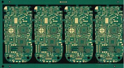
As a (quasi) PCB Layout engineer, we need to know what PCB stack-up design is, and be able to master the composition of PCB stack-up, the requirements of stack-up design, and the basic principles of PCB stack-up design. Next, let's get to know it with Banermei!
What is PCB stackup design?
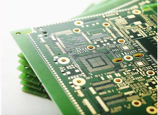
The number of layers of the PCB depends on the complexity of the circuit board. From the perspective of the PCB processing process, a multi-layer PCB is manufactured by stacking and pressing multiple "dual-panel PCBs". However, the number of layers of a multi-layer PCB, the order of stacking between the layers, and the choice of plates are determined by the circuit board designer. This is the so-called "PCB stacking design".
The composition of the PCB stack
The layer settings in the PCB design file include the following types: silk screen layer, solder mask layer, wiring layer, and plane layer.

Silk Screen: It is the physical layer where device description information and board name identification are placed on the PCB board.
Soldermask: Soldermask is an important part of the PCB. It mainly serves as a solder mask and environmental protection. The solder mask is a layer of ink attached to the surface of the PCB. Its function is to cover the PCB area that does not need to be soldered. Prevent the tin connection, while protecting the circuit from external damage to a certain extent.
Conductor: It is the physical layer that realizes the interconnection relationship between the various components of the PCB board in a "positive film" manner.
Plane: It is the physical layer that realizes each power supply and ground network connection of PCB board and provides impedance reference and return path.
Usually referred to as "stacked design", it is actually the design of the superimposed arrangement of wiring layers and plane layers.
Basic principles of PCB stackup design
PCB stacking design needs: meet the characteristic impedance requirements of the signal; meet the principle of minimizing signal loops; meet the requirements of minimizing signal interference in the PCB; meet the principle of symmetry.
Taking into account the signal quality control factors, the general principles of PCB stacking settings are as follows:
1. The second layer adjacent to the PCB component surface is the ground plane, which provides the device shielding layer and the top layer wiring to provide a reference plane.
2. All signal layers are as close as possible to the ground plane to ensure a complete return path.
3. Try to avoid the two signal layers directly adjacent to reduce crosstalk.
4. The main power supply is as close as possible to it correspondingly to form a plane capacitor to reduce the plane impedance of the power supply.
5. Taking into account the symmetry of the laminated structure, it is conducive to the warpage control during plate making.
For high-speed backplanes, the general stacking principles are as follows:
1. Top surface and Bottom surface are complete ground planes, forming a shielded cavity.
2. There is no parallel wiring of adjacent layers to reduce crosstalk, or the distance between adjacent wiring layers is much larger than the reference plane distance.
3. All signal layers are as close as possible to the ground plane to ensure a complete return path.
Reminder: In the specific PCB stacking settings, the above principles should be flexibly mastered and applied, and a reasonable analysis should be carried out according to the actual needs of the single board, and finally a suitable stacking plan should be determined.
Generally speaking, for more complex high-speed circuits, it is best not to use a four-layer board in a PCB factory because it has several unstable factors, both in terms of physical and electrical characteristics. If you must design a four-layer board, you can consider setting it as: power-signal-signal-ground. There is a better solution: the outer two layers are both grounded, and the inner two layers are used for power and signal lines. This solution is the best stacking solution for the four-layer board design. It has an excellent suppression effect on EMI and is also very beneficial to reduce the impedance of the signal line. However, the wiring space is small and it is more difficult for the board with a higher wiring density. .