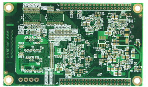
Based on your own work experience, at least a few things you need to master when learning PCB Layout:
(1) For the basic principles of circuits, please refer to "Basics of Circuit Analysis".
(2) Choose the Design tool and recommend cadence. I have also used AD. I personally feel that Cadence is more powerful and handy. And you want to take cutting-edge technology circuit boards. I don’t know how to define cutting-edge. In fact, the most challenging part of a PCB is the contradiction between design and cost Fab ability. The 24th layer), small pin pitch, narrow wiring space, demanding signal quality requirements, cumbersome wiring constraints, and a series of inspections after completion, and I believe that it will be more convenient and easy to use Cadence to complete these tasks.
(3) It is very important to use cadence to draw schematic diagrams. If you don’t know the circuit principle, it is actually difficult for you to make a good Placement (I don’t know whether this term is universal, so I’ll explain: the components of the schematic diagram are on the PCB. Actual layout), I think a good Placement actually completes more than half of a PCB design.

(4) We will make good use of the PCB space according to the schematic diagram and make a reasonable placement to ensure the best signal path and the largest signal routing space. After finishing the Placement, adjust the silk. This is the face made by the final board.
(5) Will design the PCB stackup, a reasonable and optimal (without sacrificing signal quality, taking into account the cost and wiring complexity, because the more layers, the better the line, but the higher the cost). Design the wiring constraint rules, and then complete the Layout.
(Personally, I feel that Layout is the easiest in this complete process, because under constraints, only a little experience can complete the final layout work)
(6) Know the actual Fab capabilities of the Fab manufacturer. Of course, you have to know whether your PCB is made and whether the manufacturer can produce it (if you design a 100-layer board (even if it is estimated to be a sky-high price), I don’t know which manufacturer can produce it., I currently know that the most Fab around me is only 60 multi-layers (40x60cm more than 10 W US dollars), I have not heard of 70-layers)
(7) Will make a quotation, know the charges for each Fab, stacking, blind holes, buried holes, plug holes, back drilling, machining accuracy, drilling ratio requirements, line widths, etc., which can be estimated at the beginning of the schematic Quotation, even taking the cost into consideration when designing, make the final product price competitive.
(8) After the PCB is completed, it will be inspected, including long line width inspection such as impedance matching, power line load capacity inspection, repeated wiring inspection, short circuit and open circuit inspection, signal return path inspection, etc., signal inspection, and actual Fab capability inspection, Line width inspection, line spacing, line hole spacing and so on.
(9) Generate Fab files and deliver them to Fab manufacturers.
(10) There is one point missing from the above. Regarding the BOM option, according to the schematic diagram, considering the cost and delivery cycle of the device, the impact on Placement (if they are all resistors with the same parameters, in most cases I would like to choose a small size, because Can save PCB board space) Choose the most suitable device.