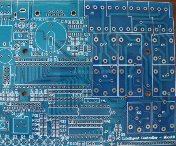
In the production process of automotive PCB boards, it is inevitable that electrical defects such as short circuits, open circuits and leakage due to external factors will inevitably be caused. In addition, automotive PCBs continue to evolve toward high density, fine pitch and multiple levels. If the defective boards are screened out and allowed to flow into the manufacturing process, it will inevitably cause more cost waste. Therefore, in addition to the improvement of process control, the improvement of testing technology can also provide PCB manufacturers with reduced scrap rate and improved product yield. solution.
In the production process of electronic products, the cost of defects caused by defects has different degrees in each stage. The earlier it is discovered, the lower the cost of remediation. "The Rule of 10's" is often used to evaluate the cost of remediation when PCBs are found to be defective at different stages of the process. For example, after the blank board is produced, if the open circuit in the board can be detected in real time, usually only need to repair the line to improve the defect, or at most one blank board is lost; but if the open circuit is not detected, wait for the board to be shipped When the downstream assembler completes the installation of the parts, the furnace tin and IR are remelted, but at this time it is detected that the circuit is disconnected. The general downstream assembler will ask the empty board manufacturing company to compensate for the cost of parts and heavy labor., Inspection fees, etc. If it is even more unfortunate, the defective board has not been found in the test of the assembler, and it enters the whole system finished product, such as computers, mobile phones, auto parts, etc. At this time, the loss discovered by the test will be the empty board in time. A hundred times, a thousand times, or even higher. Therefore, for the PCB industry, electrical testing is for early detection of circuit functional defects.

Downstream players usually require PCB manufacturers to perform 100% electrical testing, and therefore they will reach agreement with PCB manufacturers on test conditions and test methods. Therefore, both parties will first clearly define the following items:
1. Test data source and format
2. Test conditions, such as voltage, current, insulation and connectivity
3. Equipment production method and selection
4. Test chapter
5. Repair specifications
In the PCB manufacturing process, there are three stages that must be tested:
1. After the inner layer is etched
2. After the outer circuit is etched
3. Finished product
In each stage, there will usually be 2 to 3 times of 100% testing, and the defective boards will be screened out and then reworked. Therefore, the test station is also the best source of data collection for analyzing process problems. Through statistical results, the percentage of open circuits, short circuits and other insulation problems can be obtained. After heavy work, the inspection will be carried out. After the data are sorted, the quality control method can be used to find Solve the root cause of the problem.
Methods and equipment for electrical measurement
Electrical testing methods include: Dedicated, Universal Grid, Flying Probe, E-Beam, Conductive Cloth (Glue), Capacity And brush test (ATG-SCAN MAN), of which there are three most commonly used equipment, namely special test machine, general test machine and flying probe test machine. In order to better understand the functions of various devices, the following will compare the characteristics of the three main devices.
1. Dedicated test
The special test is a special test mainly because the fixture used (Fixture, such as a needle plate for electrical testing of a circuit board) is only suitable for one material number, and boards of different material numbers cannot be tested. And it cannot be recycled. In terms of the number of test points, the single panel can be tested within 10,240 points and the double-sided 8,192 points each. In terms of test density, due to the thickness of the probe head, it is more suitable for use on boards with a pitch above.
2. Universal Grid test
The basic principle of the general-purpose test is that the layout of the PCB circuit is designed according to the grid. Generally, the so-called circuit density refers to the distance of the grid, which is expressed in terms of pitch (sometimes it can also be expressed by hole density) ), and the general test is based on this principle. According to the hole position, a G10 base material is used as the mask. Only the probe at the hole position can pass through the mask for electrical testing. Therefore, the manufacture of the fixture is simple and fast, and the probe The needle can be reused. General-purpose test has a standard Grid fixed large needle plate with extremely many measuring points. The needle plates of the movable probe can be made according to different material numbers. When mass production, the movable needle plate can be changed to mass production for different material numbers. test.
In addition, in order to ensure the smoothness of the completed PCB board circuit system, it is necessary to use a high-voltage (such as 250V) multi-point general-purpose electrical test master machine to conduct an Open/Short electrical test on the board with a needle plate with a specific contact. This kind of universal testing machine is called "automated testing machine".
The general-purpose test points are usually more than 10,000 points, and the test with a test density or is called an on-grid test. If it is applied to a high-density board, it is out of on-grid design due to too close spacing, so it belongs to off-grid For testing, the fixture must be specially designed, and the test density of general-purpose testing is usually up to QFP.
3. Flying Probe Test
The principle of flying probe test is very simple. It only needs two probes to move x, y, z to test the two end points of each circuit one by one, so there is no need to make additional expensive jigs. However, because it is an end point test, the test speed is extremely slow, about 10-40 points/sec, so it is more suitable for samples and small mass production; in terms of test density, flying probe test can be applied to extremely high-density PCB boards.