PCB schematic component design
If there are required components in the PROTEL component library, you can directly find out and put them in the schematic diagram. If there is no required component, you need to create a new principle component library (Sch.lib). Process: In the original In the component library, find the component 1 with the same (or similar) number of pins as the required component. When the cursor becomes a cross cursor, move the cursor to the component, click the mouse to determine a reference point. Then switch to the Sch.lib file to be edited, and create a new device (shortcut creat component) in the file and modify it Name. Click SCH Lib in the lower right corner of the environment, move the mouse cursor to the empty component name, click the right mouse button, and execute in the pop-up shortcut menu
Paste command, paste the component 1 into the newly created component library. Then modify the pin properties. Then execute the menu command Report|Component Rule Check to perform the regulatory inspection.

2. PCB schematic design
Create a new PCB schematic file-->load the component library (including loading the component library you created)-->place the component-->the schematic wiring output device report<--correct the error--comile all projects<-set the compilation error first Report option (Reports/Bills of Materials) output network report (if there is no hierarchical schematic diagram, you can only generate a single document network report Design/NetlistForDocument/Protel, if there is a hierarchical module diagram, you need to generate a project network report (Protel) In the schematic design, if the circuit diagram is more complicated, you can use the hierarchical schematic design from top to bottom (or bottom to top).
3. Component PCB packaging design
You can use a component of the same (or similar) package to perform simple attribute modification to obtain the required component package. The specific operation process is the process of copying and modifying the component package from .pcbdoc to .PCBlib. No longer here. Go into details. No registration required
After the component package is modified, execute Edit/Set Preference/pin 1 to set the package reference point at the first pin. Then execute Report/Component Rule check to set all the rules to be checked, and OK. At this point, the package is established.
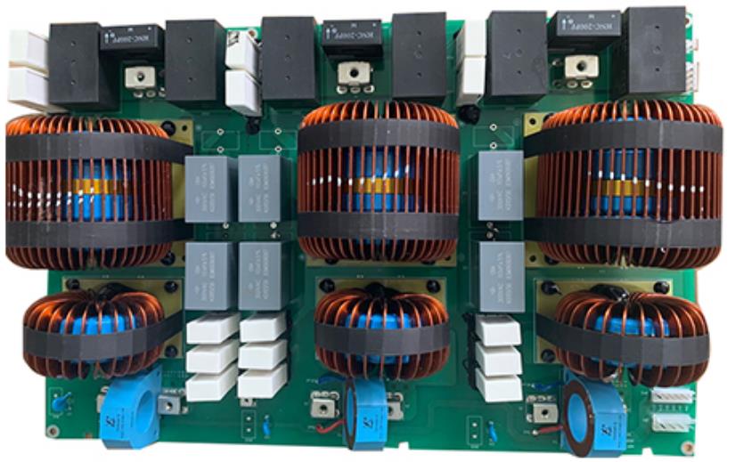
4. PCB design
First create a new PCB file, and import the network table when the package lib has been loaded.
Automatic component layout. Before this step, you must first set the size of the PCB, you have to plan the size and shape for him. Click on the bottom to select keep-out layer, and then in the place menu, select Draw Line, and then draw a rectangle on the black baseboard. You can choose the size.
Note: The line drawn at this time is pink! This shows that you are planning the size of the circuit board in the keep-out layer. Then automatic layout, routing can proceed smoothly.
No matter what software is used, there is a general procedure for PCB design, which will save time and effort in order, so I will introduce it according to the production process.
Schematic design is the preliminary work. It is often seen that beginners directly draw PCB boards in order to save trouble. This will not pay off. For simple boards, if you are familiar with the process, you can skip it. But for beginners, you must follow the process, so that on the one hand, you can develop good habits, and on the other hand, the only way to avoid mistakes for complex circuits.
When drawing a schematic diagram, pay attention to the final connection of each file into a whole when designing the hierarchy, which is also of great significance for future work. Due to differences in software, some software may appear to be connected but not connected (in terms of electrical performance). If you don’t use related testing tools, in case something goes wrong, it’s too late to find out when the board is ready. Therefore, the importance of doing things in order has been repeatedly emphasized, and I hope to attract everyone's attention.
The schematic diagram is based on the designed project, as long as the electrical connection is correct, there is nothing to say.