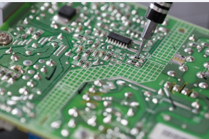
First, the overlap of PCB pads
1. Overlapping pads (except for surface paste pads) means that the holes overlap. During the PCB drilling process, multiple drills will drill holes on multiple drills, causing damage to the holes.
2. The two holes of the multilayer board overlap. For example, one hole is the isolation disk, and the other hole is the connection disk (flower pad), which will cause the performance of the separation disk after the membrane to be scrapped.
two. Misuse of graphics layers
1. Do some useless wiring on some graphics layers. The original four-layer line but the design of more than five-layer lines will cause misunderstandings.
2. Save the design time diagram. Take the Protel software as an example. Each layer line is drawn together with the board layer, and the line is marked with the board layer. In this way, when the light draws the data, because the board layer is not a choice, lack of connections and circuit breakers, or due to selection The circuit board layer with marked lines and short circuits is removed. Therefore, the design of the graphics layer should maintain integrity and clarity.

3. Violation of conventional design, such as the surface design of the bottom element, and the welding surface design on the top, causing inconvenience.
three. Disorderly release characters
1. The character cover pad SMD solder brings inconvenience to the printed board passing test and component soldering.
2. The character design is too small, making screen printing difficult, and the Congress also makes it difficult to distinguish the characters from overlapping each other.
Four. The PCB is set with the aperture 1 of the single-sided pad, and the single-sided pad is generally not drilled. If the drilling needs to be marked, the aperture should be designed to be zero.
If a numerical value is designed, the coordinates of the hole will appear at this position when the drilling data is generated, and there is a problem.
2. Drill holes such as single-sided welded plates should be specially labeled.
V. Draw a pad with padding
The pads drawn on the design line with filler blocks can pass DRC inspection, but processing is impossible, so the type of pads cannot directly generate resistance welding data. In the resistance flux, the pad area will be blocked by flux, resulting in Difficulty in welding equipment.
Sixth, the PCB electronic layer is also a flower pad and connection. Because the power supply is designed as a flower pad, the image formed is contrary to the actual printed board. All connections are isolated lines, and the designer should be very clear.
By the way, be careful when drawing several sets of power supplies or a few pieces of land. Do not leave gaps so that the two sets of power supplies will not be short-circuited, and the connection area will not be blocked (allowing a set of power supplies to be separated).
seven. The definition of the processing level is unclear
1. The single-layer board is designed on the top layer. If the front and back sides are not explained, the board produced may not be well welded when installed on the equipment.
2. For example, a four-layer design uses the top mid1 and mid2 bottom four layers, but the processing is not placed in this order, which needs clarification.
Eight. Too many fillers in PCB design or fillers with very fine lines
1. The production of light drawing data is lost, and the light drawing data is incomplete.
2. Because the filling block in the light drawing data processing is drawn by a line, the amount of light drawing data generated is quite large, which increases the difficulty of data processing.
Nine, the soldering board of the surface mount device is too short
This is used to pass the test. For too dense surface mount equipment, the spacing between the two feet is very small, and the pad is also very fine. The installation of the test pin must be staggered up and down (left and right), such as the mat design is too short, although it It will not affect the installation of the equipment, but it will make the test needle wrong.
Ten, the large area of the grid is too small
The large-area grid lines formed between the edges of the lines are too small (less than 0.3mm). In the manufacturing process of the printed circuit board, the drawing process can easily produce a large number of broken films attached to the circuit board after the display, resulting in disconnection .
11. The distance between the large area copper foil and the outer frame is too close
The distance between the large area of copper foil and the frame should be at least 0.2mm, because when milling shapes, such as milling to copper foil, it is easy to cause copper foil warpage and the problem of flux shedding caused by it.
12. The shape of the frame design is not clear
Some customers who keep the PCB layer, PCB board layer, top layer, etc. have designed the shape of the line, these shape lines do not overlap, resulting in PCB m