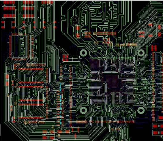
1. PCB printed board screen
The screen is the most important part of the PCB design, because it is the key to controlling the fluidity of the ink and the thickness of the printing. At the same time, it determines the durability of the screen and the wide application of the quality switch manufacturing technology. In addition, the excellent combination of screen and screen photosensitive materials is also an important factor in the production of high-quality, high-precision screen printing plates. In order to ensure a good combination of the screen and the photosensitive material, the traditional method is to roughen and degrease the new screen, which can ensure the quality of the screen and prolong the service life of the screen.
2.PCB printed board screen frame
The material of the screen frame and the shape of the cross section are very important. Compared with a certain size of screen frame, if the strength of the screen frame is not enough, the uniformity of tension cannot be guaranteed. Nowadays, high-tension aluminum frame is generally used.
3. PCB printed board printing plate photosensitive material

Commonly used photosensitive materials for printing plates are diazo sensitizers and photosensitive films. Diazo emulsions are commonly used in the production of screen printing screens. The photosensitive film has the characteristics of uniform and controllable film thickness, high resolution, high definition, wear resistance, and strong adhesion to the screen, and has been widely used in the character printing of printed boards.
4. PCB printed board screen printing ink
The following mainly introduces some of the screen printing inks used in the PCB industry,
Second, the application of the solder mask on the PCB surface
The solder mask of the printed circuit board is a permanent protective layer, which not only has the functions of anti-soldering, protection, and improvement of insulation resistance, but also has a great influence on the appearance of the circuit board. In the early days of solder mask printing, a solder mask film was first used to make a screen pattern, and then UV light-curable solder mask ink was printed. After each printing, the excess solder mask remains on the pad due to the deformation of the screen and the inaccurate positioning. It takes a long time to scrape off, which consumes a lot of manpower and time. Liquid photosensitive solder resist ink does not need to produce screen graphics, and uses air-screen printing and contact exposure. This process has high alignment accuracy, strong solder mask adhesion, good solder resistance, and high production efficiency. It has gradually replaced light solid inks.
1PCB printed board. Process flow
Making solder mask film - punching the positioning holes of the film - cleaning the printed board - preparing ink - double-sided printing - pre-baking - exposure - developing - thermosetting
2. PCB printed board key process analysis
(1)PCB printed board pre-baking
The purpose of pre-bake is to evaporate the solvent contained in the ink and make the solder resist film into a non-stick state. For different inks, the temperature and time of pre-bake are different. If the pre-bake temperature is too high, or the drying time is too long, it will cause poor development and reduce the resolution; if the pre-bake time is too short or the temperature is too low, the film will stick during exposure, and the solder mask will be exposed to sodium carbonate solution during development. Corrosion, causing the surface to lose luster or the solder mask to swell and fall off.
(2) PCB printed board exposure
Exposure is the key to the entire process. For positive images, when overexposed, due to the scattering of light, the solder mask at the edge of the pattern or line reacts with light (mainly the photosensitive polymer contained in the solder mask reacts with light), resulting in a residual film, which reduces the resolution, Resulting in smaller developed graphics and thinner lines; if exposed
When it is insufficient, the result is contrary to the above-mentioned situation, and the developed pattern becomes larger and the line becomes thicker. This situation can be reflected by the test: if the exposure time is long, the measured line width is a negative tolerance; if the exposure time is short, the measured line width is a positive tolerance. In the actual process, a "light energy integrator" can be used to determine the best exposure time.
(3) PCB printed board ink viscosity adjustment
The viscosity of the liquid photosensitive solder resist ink is mainly controlled by the ratio of the hardener to the main agent and the addition amount of the diluent. If the amount of hardener added is not enough, an imbalance of ink characteristics may occur. After the hardener is mixed, it reacts at room temperature, and its viscosity changes as follows.
30min~10h: The ink main agent and hardener have been fully fused, and the fluidity is proper.
Within 30min: The ink main agent and hardener have not been fully fused, the fluidity is not enough, and the screen will be blocked during printing.
After 10h: The reaction between the various materials of the ink itself has been actively proceeding, resulting in increased fluidity and poor printing. The longer the hardener is mixed, the more fully the reaction between the resin and the hardener will be, and the gloss of the ink will also change. good. In order to make the ink gloss uniform and printability good, it is best to put the hardener for 30 minutes to start printing.
If the thinner is added too much, it will affect the heat resistance and hardenability of the ink. In a word, the viscosity adjustment of liquid photosensitive solder mask ink is very important: the viscosity is too thick, and the screen printing is difficult. The screen is easy to stick to the screen; the viscosity is too thin, and the amount of volatile solvent in the ink is large, which brings difficulties to the pre-curing.
The viscosity of the ink is measured with a rotary viscometer. In production, the best value of viscosity must be adjusted according to different inks and solvents.
Third, the application of anti-corrosion and anti-electroplating layer in the process of PCB pattern transfer
In the manufacturing process of printed boards, pattern transfer is a key process. In the past, dry film technology was commonly used to transfer printed circuit patterns. Now, wet film is mainly used for the production of inner circuit patterns of multilayer printed boards and the production of outer circuit patterns of double-sided and multilayer boards.
1. PCB process
Pre-treatment - screen printing - baking - exposure - development - anti-plating or anti-corrosion - film removal - next process
2. PCB printed board key process analysis
(1) The choice of coating method for PCB printed board
Wet film coating methods include screen printing, roll coating, curtain coating, and dip coating.
Among these methods, the wet film surface film layer produced by the roller coating method is not uniform, which is not suitable for making high-precision printed boards; the wet film surface film layer produced by the curtain coating method is uniform and the thickness can be accurately controlled, but Curtain coating equipment is expensive and suitable for mass production; the wet film surface film thickness produced by the dip coating method is thinner and has poor electroplating resistance. According to current PCB production requirements, screen printing methods are generally used for coating.
(2) PCB pre-processing
The adhesion of the wet film and the printed board is completed by chemical bonding. Usually the wet film is a polymer with acrylate as the basic component. It is through the free movement of unpolymerized acrylate groups and copper Combine. This process adopts the method of chemical cleaning and then mechanical cleaning to ensure the above-mentioned bonding effect, so that the surface is free of oxidation, oil stains, and water marks.