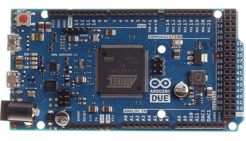
When it comes to PCB boards, many friends will think that it can be seen everywhere around us, from all household appliances, various accessories in computers, to various digital products, as long as they are electronic products almost all use PCB boards, so what exactly is it? What about the PCB board? The PCB board is the PrintedCircuitBlock, the printed circuit board, for the placement of electronic components, and the base version with circuits. By using a printing method, the copper-plated base plate is printed on the anti-corrosion circuit, and the circuit is etched and washed out.
PCB boards can be divided into single-layer boards, double-layer boards and multi-layer boards. Various electronic components are integrated on the PCB. On the most basic single-layer PCB, the parts are concentrated on one side, and the wires are concentrated on the other side. In this case, we need to make holes in the board so that the pins can pass through the board to the other side, so the pins of the parts are soldered to the other side. Because of this, the front and back sides of such a PCB are called the component side (ComponentSide) and the solder side (SolderSide) respectively.

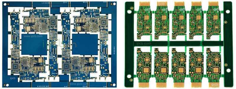
The double-layer board can be regarded as a combination of two single-layer boards relative to each other. There are electronic components and wiring on both sides of the board. Sometimes it is necessary to connect a single wire on one side to the other side of the board, which requires a via. A via is a small hole filled or coated with metal on the PCB, which can be connected with the wires on both sides. Many computer motherboards now use 4-layer or even 6-layer PCB boards, while graphics cards generally use 6-layer PCB boards. Many high-end graphics cards like the nVIDIAGeForce4Ti series use 8-layer PCB boards. This is the so-called multi-layer PCB board. The problem of connecting the lines between the various layers will also be encountered on a multilayer PCB, which can also be achieved through vias.
Because it is a multi-layer PCB, sometimes the vias do not need to penetrate the entire PCB. Such vias are called Buriedvias and Blindvias, because they only penetrate a few layers. Blind holes are to connect several layers of internal PCB to the surface PCB, without having to penetrate the entire board. Buried vias only connect to the internal PCB, so they cannot be seen from the surface. In a multilayer PCB, the entire layer is directly connected to the ground wire and the power supply. So we classify each layer as signal layer, power layer or ground layer. If the parts on the PCB require different power supplies, this type of PCB usually has more than two layers of power and wire. The more PCB layers used, the higher the cost. Of course, the use of more layers of PCB boards is very helpful to provide signal stability.
The professional PCB board production process is quite complicated, take a 4-layer PCB board as an example. The main board PCB is mostly 4-layer. When manufacturing, the two middle layers are rolled, cut, etched, and oxidized. The four layers are the component surface, power layer, ground layer, and solder pressure layer. Put these 4 layers together and roll them into a motherboard PCB. Then punch and make through holes. After cleaning, print, copper, etch, test, solder mask, silk screen on the outer two layers of circuits. Finally, the entire PCB (including many motherboards) is stamped into a motherboard PCB, and then vacuum packaged after passing the test. If the copper is not well laid during the PCB manufacturing process, there will be a phenomenon of loose bonding, which is likely to imply short circuit or capacitive effect (easy to produce interference). The vias on the PCB must also be paid attention to. If the hole is not in the middle, but to one side, uneven matching will occur, or it will be easy to contact the power layer or ground layer in the middle, which will cause potential short circuits or poor grounding factors.
Copper wiring process
The first step is to establish the wiring between the parts. We use negative film transfer method to show the working film on the metal conductor. This technique is to spread a thin layer of copper foil on the entire surface and eliminate the excess. Supplementary transfer is another method that less people use. It is a method of laying copper wires only where needed, but we won't talk about it here.
Positive photoresist is made of sensitizer, which will dissolve under lighting. There are many ways to treat the photoresist on the copper surface, but the most common way is to heat it and roll it on the surface containing the photoresist. It can also be sprayed on the head in a liquid way, but the dry film type provides higher resolution and can also produce thinner wires. The hood is just a template for the PCB layer in manufacturing. Before the photoresist on the PCB board is exposed to UV light, the light shield covering it can prevent the photoresist in some areas from being exposed. These areas covered by photoresist will become wiring. After the photoresist is developed, the other bare copper parts to be etched. The etching process can immerse the board in the etching solvent or spray the solvent on the board. Generally used as an etching solvent, ferric chloride and the like are used. After the etching, the remaining photoresist is removed.