The innovation of printed circuit, first of all lies in the innovation of PCB products and the market.
The innovation of printed circuits is based on technological innovation. Noisy Printed Electronic Circuits (PEC) has brought revolutionary changes to PCB products and production processes.
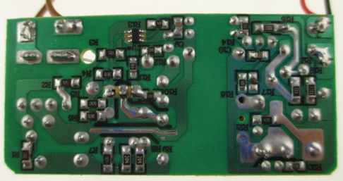
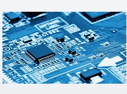
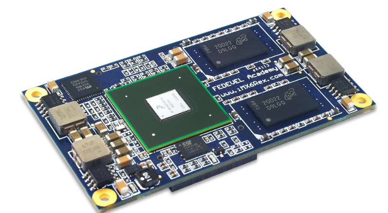
Printed circuit board (PCB) has become an indispensable accessory of modern electronic equipment. No matter the high-end electronic equipment in the world, or household appliances and electronic toys, PCBs that load electronic components and electrical signals are indispensable, and PCBs follow the entire Developed by the development of the electronic information industry.
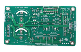
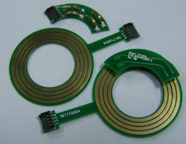
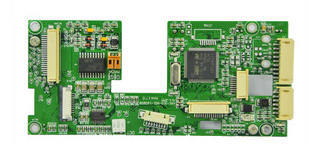
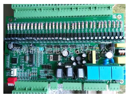
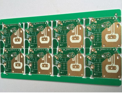
The innovation of printed circuit, first of all lies in the innovation of PCB products and the market. The earliest PCB products were single-sided boards with only one layer of conductors on the insulating board, and the circuit width was measured in millimeters, which was commercialized in semiconductor (transistor) radios. Later, with the advent of televisions and computers, PCB products were innovated, and double-sided and multi-layer boards appeared. There were two or more layers of conductors on the insulating board, and the line width was gradually reduced. In order to adapt to the miniaturization and lightweight development of electronic equipment, flexible PCBs and rigid-flex PCBs have emerged.

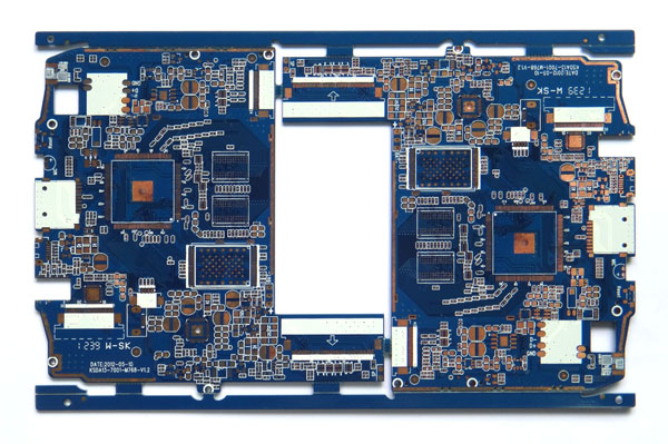
At present, the main PCB markets are in the fields of computers (computers and peripherals), communication equipment (base stations and handheld terminals, etc.), home electronics (TVs, cameras, game consoles, etc.), and automotive electronics. PCB products are multi-layer boards and High-density interconnect (HDI) boards are the main ones. With the development of computers to high-speed and large-capacity, mobile phones to multi-functional intelligence, TVs to high-definition 3D, and automobiles to high-security and intelligent development, HDI printed boards have also changed from wire connection functions to electronic circuit functions., That is, in addition to basic conductor lines, PCB products also include passive components such as resistors and capacitors and active components such as IC chips. The new generation of HDI printed boards are embedded component printed boards with internal components. The newer generation of printed boards is suitable for high-frequency and high-speed signal transmission applications. The PCB layers will contain optical fibers and waveguides to form photoelectric printed boards suitable for signal transmission above 40GHz.
It is precisely because of the continuous innovation of PCB products that we usher in the spring of printed circuit development one after another. Smart phones will bring the climax of embedded component printed boards, LED energy-saving lighting will bring the climax of metal-based printed boards, and e-books and thin-film displays will bring the climax of flexible circuit boards.
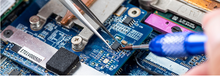
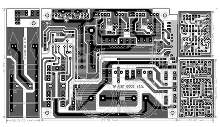
The innovation of printed circuits is based on technological innovation. The traditional technology of PCB manufacturing is the copper foil etching method (subtractive method), that is, the copper-clad insulating substrate is etched by a chemical solution to remove the unnecessary copper layer, leaving the required copper conductor to form the circuit pattern; for double-sided and multi-layered The interconnection between the layers of the board is realized by drilling and electroplating copper. At present, this traditional process has been difficult to adapt to the production of micron-level fine-line HDI boards, and it is difficult to achieve rapid and low-cost production, and it is difficult to achieve the goals of energy saving, emission reduction, and green production. Only technological innovation can change this situation.
High density is the eternal theme of PCB technology. High-density features are thinner lines, smaller interconnection holes, higher number of layers, and lighter weight. For example, the conventional line width/line spacing capability of PCBs has been refined from 100μm to 75μm and 50μm, and will be refined to 25μm and 20μm in a few years. Therefore, the copper foil etching process must be reformed and innovated.
For the technological innovation of printed circuits, people have been pursuing semi-additive and additive technologies, that is, depositing a copper layer on an insulating substrate to form a circuit pattern. This is an improvement on the traditional subtractive method. Although there is progress, it still needs a lot of Energy consumption, and the cost is also high. The new path of innovation is printed electronic circuits (PEC), which has brought revolutionary changes to PCB products and production processes. Printed electronic circuit technology uses a pure printing method to realize electronic circuit graphics, that is, screen printing, offset printing or inkjet printing technology is used to print functional inks (conductive inks, semiconductor inks, insulating inks, etc.) on insulating substrates On, get the required electronic circuit. This technology can simplify the production process, save raw materials, reduce pollutants, and reduce production costs. If equipped with Roll to Roll processing equipment, it can achieve mass and low-cost production.
The continuous development of printed electronic circuit technology will bring the PCB industry to a higher level.