Since the large-scale industrial production of flexible printed circuit boards (FPC), it has experienced more than 30 years of development. In the 1970s, FPC began to enter the mass production of real industrialization. Development to the late 1980s, due to the advent and application of a new type of polyimide film material, the FPC appeared without adhesive type FPC (generally referred to as "two-layer FPC"). In the 1990s, the world developed a photosensitive cover film corresponding to high-density circuits, which caused a great change in the design of FPC. Due to the development of new application areas, the concept of its product form has undergone a lot of changes, and it has been extended to include a larger range of substrates for TAB and COB. The high-density FPC that emerged in the second half of the 1990s began to enter large-scale industrial production. Its circuit pattern has rapidly developed to a more subtle level. The market demand for high-density FPC is also growing rapidly.

At present, the annual output value of FPC produced in the world has reached approximately US$3 billion to US$3.5 billion. In recent years, the output of FPC in the world has been increasing. Its proportion in PCB is also increasing year by year. In the United States, *** and other countries, FPC accounts for 13%-16% of the total output value of printed circuit boards. FPC has increasingly become a very important and indispensable variety in PCB.
In terms of flexible copper clad laminates, there is a big gap between China and advanced countries and regions in the production scale, manufacturing technology level and raw material manufacturing technology, and this gap is even greater than that of rigid copper clad laminates.
Copper clad laminates should develop simultaneously with PCB
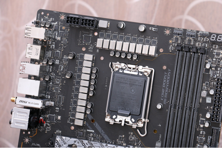
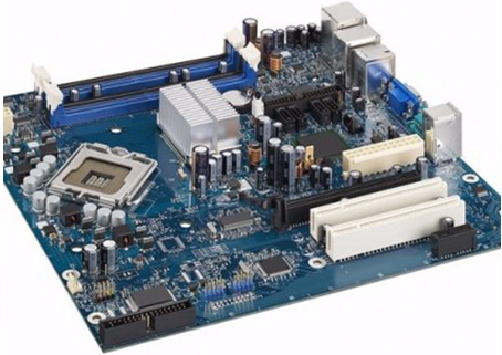
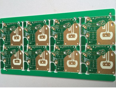
Copper clad laminate (CCL), as the substrate material in PCB manufacturing, mainly plays the role of interconnection, insulation and support for PCB, and has a great impact on the transmission speed, energy loss, characteristic impedance, etc. of the signal in the circuit. Therefore, PCB The performance, quality, processability in manufacturing, manufacturing level, manufacturing cost, and long-term reliability and stability of CCL depend to a large extent on the material of the copper clad laminate.
CCL technology and production have gone through more than half a century of development. Now the world's annual output of CCL has exceeded 300 million square meters, and CCL has become an important part of basic materials in electronic information products. The copper clad laminate manufacturing industry is a sunrise industry. It has broad prospects along with the development of electronic information and communication industries. Its manufacturing technology is a high-tech that intersects, penetrates, and promotes multiple disciplines. The development history of electronic information technology shows that copper clad laminate technology is one of the key technologies that promote the rapid development of the electronics industry.
The development of copper clad laminate technology and production and the electronic information industry, especially the development of the PCB industry are synchronized and inseparable. This is a process of continuous innovation and continuous pursuit. The progress and development of copper clad laminates are constantly driven by the innovation and development of electronic products, semiconductor manufacturing technology, electronic mounting technology, and PCB manufacturing technology.
The rapid development of the electronic information industry has enabled electronic products to develop in the direction of miniaturization, functionalization, high performance, and high reliability. From the general surface mount technology (SMT) in the mid-1970s to the high-density interconnect surface mount technology (HDI) in the 1990s, as well as the application of various new packaging technologies such as semiconductor packaging and IC packaging technology that have emerged in recent years, Electronic installation technology continues to develop in the direction of high density. At the same time, the development of high-density interconnect technology promotes the development of PCBs in the direction of high density. With the development of mounting technology and PCB technology, the technology of copper clad laminate as a PCB substrate material is also constantly improving.