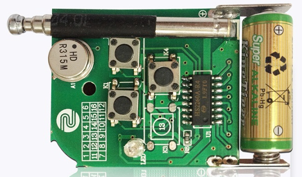
The anti-interference design of the printed circuit board has a close relationship with the specific circuit. Here only a few common anti-interference measures in the PCB design will be explained.
1. Power cord design:
According to the current of the printed circuit board, try to increase the width of the power line to reduce the loop resistance. At the same time, make the direction of the power line and ground line consistent with the direction of data transmission, which helps to enhance the anti-noise ability.
2. Principles of ground wire design:

(1) The digital ground is separated from the analog ground. If there are both logic circuits and linear circuits on the circuit board, they should be separated as much as possible. The ground of the low-frequency circuit should be grounded in parallel at a single point as much as possible. When the actual wiring is difficult, it can be partially connected in series and then grounded in parallel. The high-frequency circuit should be grounded at multiple points in series, the ground wire should be short and leased, and the grid-like large-area ground foil should be used around the high-frequency component as much as possible.
(2) The grounding wire should be as thick as possible. If the ground wire uses a very tight line, the ground potential changes with the change of the current, which reduces the anti-noise performance. Therefore, the ground wire should be thickened so that it can pass three times the allowable current on the printed board. If possible, the grounding wire should be 2~3mm or more.
(3) The ground wire forms a closed loop. For printed boards composed only of digital circuits, most of their grounding circuits are arranged in loops to improve noise resistance.
3. Decoupling capacitor configuration:
One of the conventional methods of PCB layout design is to configure appropriate decoupling capacitors on each key part of the printed circuit board. The general configuration principles of decoupling capacitors are:
(1) The power input terminal is connected with a 10~100uf electrolytic capacitor. If possible, it is better to connect to 100uF or more.
(2) In principle, each integrated circuit chip should be equipped with a 0.01pF ceramic capacitor. If the gap of the printed board is not enough, a 1-10pF tantalum capacitor can be arranged for every 4~8 chips.
(3) For devices with weak anti-noise ability and large power changes when shutting down, such as RAM and ROM storage devices, a decoupling capacitor should be directly connected between the power line and the ground line of the chip.
(4) Capacitor leads should not be too long, especially for high frequency bypass capacitors.
(5) When there are contactors, relays, buttons and other components in the PCB circuit board. When operating them, large spark discharges are generated, and RC circuits must be used to absorb the discharge current. Generally, R is 1~2K, and C is 2.2~47UF.
(6) The input impedance of CMOS is very high and it is susceptible to induction, so the unused terminal should be grounded or connected to a positive power supply when in use.