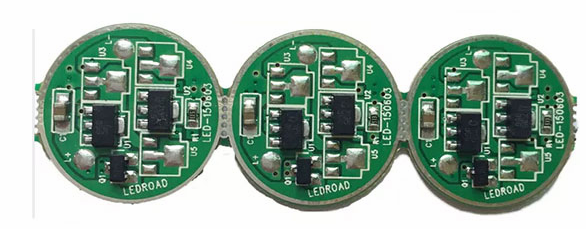
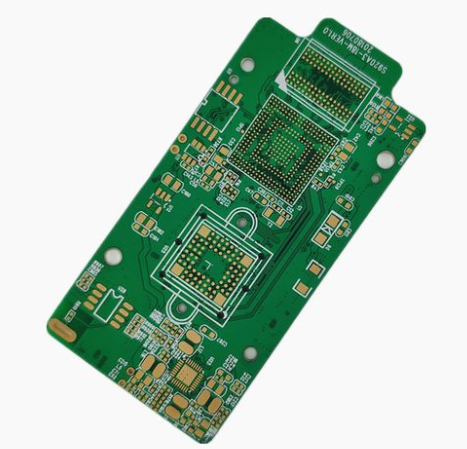
At present, electronic equipment is still used in various electronic equipment and systems with printed circuit boards as the main assembly method. Practice has proved that even if the circuit schematic design is correct and the printed circuit board is not properly designed, it will adversely affect the reliability of electronic equipment. For example, if two thin parallel lines of the printed board are close together, it will cause a delay in the signal waveform, and reflection noise will be formed at the end of the transmission line. Therefore, when designing a printed circuit board, care should be taken to adopt the correct method.
1. Ground wire design

In electronic equipment, grounding is an important method to control interference. If the grounding and shielding can be properly combined and used, most of the interference problems can be solved. The ground structure of electronic equipment roughly includes system ground, chassis ground (shield ground), digital ground (logical ground), and analog ground. The following points should be paid attention to in the ground wire design:
1. Correctly choose single-point grounding and multi-point grounding
In the low-frequency PCB circuit, the working frequency of the signal is less than 1MHz, its wiring and the inductance between the devices have little influence, and the circulating current formed by the grounding circuit has a greater influence on the interference, so one point grounding should be adopted. When the signal operating frequency is greater than 10MHz, the ground wire impedance becomes very large. At this time, the ground wire impedance should be reduced as much as possible, and the nearest multiple points should be used for grounding. When the working frequency is 1~10MHz, if one-point grounding is adopted, the length of the ground wire should not exceed 1/20 of the wavelength, otherwise the multi-point grounding method should be adopted.
2. Separate the digital circuit from the analog circuit
There are both high-speed logic circuits and linear circuits on the PCB circuit board. They should be separated as much as possible, and the ground wires of the two should not be mixed, and they should be connected to the ground wires of the power supply terminal. Try to increase the grounding area of the linear circuit as much as possible.
3. Make the ground wire as thick as possible
If the ground wire is very thin, the ground potential will change with the current change, causing the timing signal level of the electronic device to be unstable and the anti-noise performance to deteriorate. Therefore, the grounding wire should be as thick as possible so that it can pass the allowable current on the printed circuit board. If possible, the width of the ground wire should be greater than 3mm.
4. Form the ground wire into a closed loop
When designing the ground wire system of the PCB circuit board composed of only digital circuits, making the ground wire into a closed loop can significantly improve the anti-noise ability. The reason is that there are many integrated circuit components on the printed circuit board, especially when there are components with high power consumption, due to the limitation of the thickness of the ground wire, a large potential difference will be generated on the ground junction, which will cause the anti-noise ability to decrease, If the grounding structure is formed into a loop, the potential difference will be reduced and the anti-noise ability of electronic equipment will be improved.