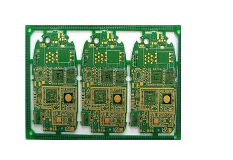
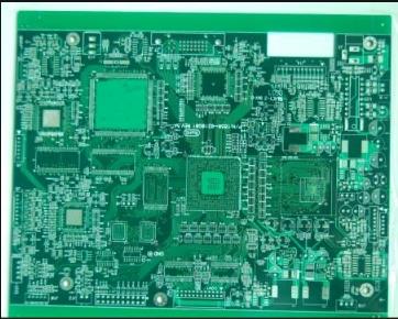
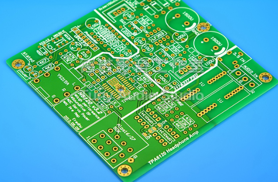
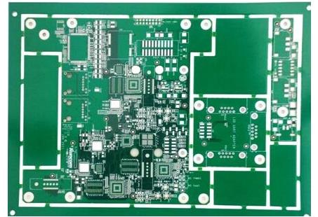
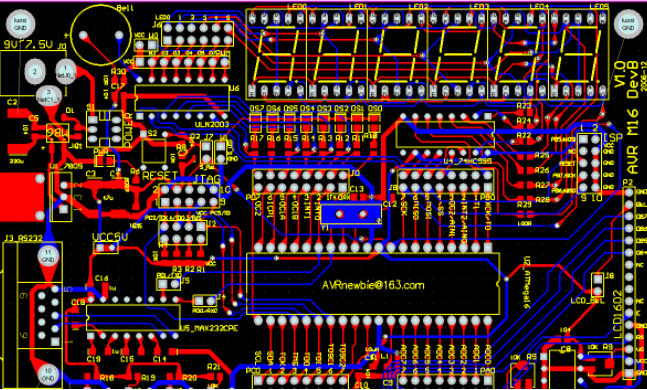
The PCB board is very common in our daily life. If there is a problem, the whole electrical appliance will not be used, so today I will tell you how to check the PCB board.
1. Manual visual inspection of PCB board
Use a magnifying glass or a calibrated microscope, and use the operator's visual inspection to determine whether the circuit board is qualified or not, and to determine when a correction operation is required.
Advantages: low up-front cost and no test fixture;
Disadvantages: At present, due to the increase in PCB production and the shrinking of PCB wire spacing and component volume, this method has become increasingly infeasible;
2. PCB board online test
Through electrical performance testing to find manufacturing defects and test analog, digital and mixed-signal components to ensure that they meet specifications, there are several testing methods such as bed-of-needle testers and flying probe testers.
Advantages: low test cost for each board, strong digital and functional testing capabilities, fast and thorough short-circuit and open-circuit testing, programming firmware, high defect coverage and easy programming, etc.
Disadvantages: Need to test fixtures, programming and debugging time, high cost of making fixtures, and difficult to use.

3. PCB board function test
The functional system test is to use special test equipment in the middle stage and the end of the production line to conduct a comprehensive test on the functional modules of the circuit board to confirm the quality of the circuit board.
4. Automatic optical inspection
Also known as automatic visual inspection, it is based on optical principles and comprehensively uses multiple technologies such as image analysis, computer and automatic control to detect and deal with defects encountered in production. It is a relatively new method of confirming manufacturing defects.
5. Automatic X-ray inspection
Taking advantage of the difference in X-ray absorptivity of different substances, defects can be found in the parts that need to be inspected through fluoroscopy. It is mainly used to detect defects in ultra-fine pitch and ultra-high-density circuit boards, as well as bridging, missing chips, poor alignment, and other defects generated during the assembly process. It can also use its tomographic imaging technology to detect internal defects in IC chips. It is currently the only method to test the soldering quality of the ball grid array and the blocked solder balls
Advantages: able to detect BGA welding quality and embedded components, high-precision product internal conditions;
Disadvantages: high cost;
6. Laser detection systemIt is the latest development of PCB testing technology. It uses a laser beam to scan the printed board, collects all measurement data, and compares the actual measurement value with the preset qualified limit value. This technology has been proven on the bare board and is being considered for assembly board testing, and the speed is sufficient for mass production lines.
Advantages: fast output, no fixture and visual non-covered access;
Disadvantages: high initial cost, maintenance and use problems are its main disadvantages;