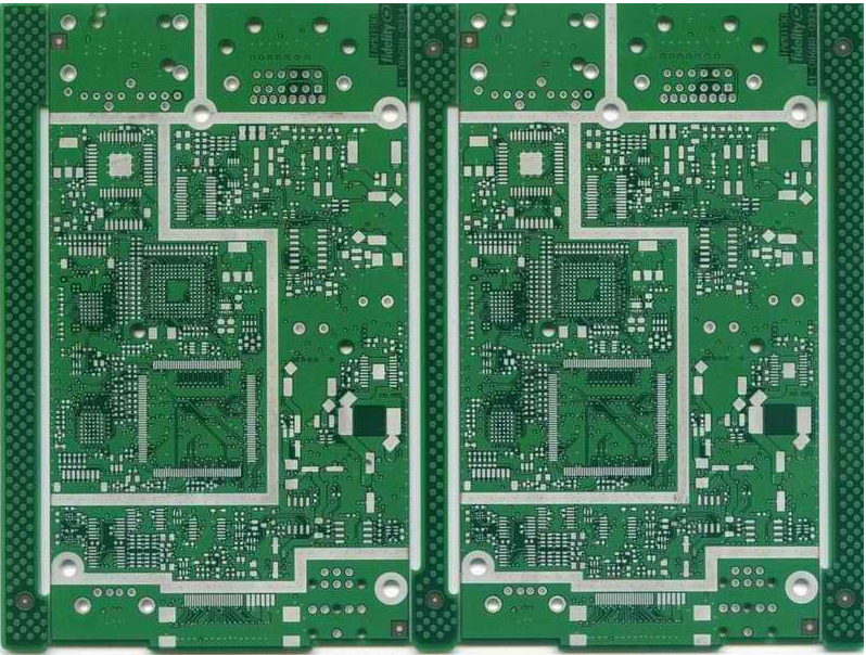
Printed circuit board (PCB) will appear in almost every electronic device. If there are electronic parts in a certain device, they are all mounted on PCBs of different sizes. In addition to fixing various small parts, the main function of the PCB is to provide electrical connections between the upper parts. As electronic devices become more and more complex, more and more parts are needed, and the circuits and parts on the PCB are becoming more and more dense. The standard PCB looks like this. The bare board (no parts on it) is often called "PrintedWiringBoard (PWB)".
1. Common mistakes in PCB schematics:
(1) There is no signal connected to the ERC report pin:

b. Inconsistent grid attributes are modified when components are created or placed, and the pins and wires are not connected;
c. When creating the component, the pin direction is reversed, and the non-pin name end must be connected.
(2) The component went out of the drawing boundary: no component was created in the center of the diagram paper of the component library.
(3) The network table of the created project file can only be partially imported into the PCB: when the netlist is generated, global is not selected.
(4) When using multi-part components created by yourself, never use annotate.
2. Common errors in PCB:
(1) It is reported that NODE is not found when loading the network:
a. The components in the original PCB image use packages that are not in the PCB library;
b. The components in the PCB schematic diagram use packages with inconsistent names in the PCB library;
c. The components in the PCB schematic diagram use packages with inconsistent pin numbers in the PCB library. For example, a triode: the pinnumbers in sch are e, b, c, and the pin numbers in PCB are 1, 2, 3.
(2) It can't always be printed on one page when printing:
a. It is not at the origin when creating the PCB library;
b. The components have been moved and rotated many times, and there are hidden characters outside the boundaries of the PCB board. Select to show all hidden characters, reduce the PCB, and then move the characters to the boundary.
(3) The DRC reporting network is divided into several parts:
Indicates that this network is not connected. Look at the report file and use CONNECTEDCOPPER to find it.
In addition, remind friends to use WIN2000 as much as possible to reduce the chance of blue screen; export the file several times to make a new DDB file to reduce the file size and the chance of PROTEL freezing. If you make a more complicated design, try not to use automatic wiring.
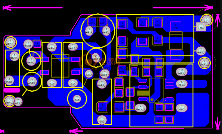
In PCB design, wiring is an important step to complete product design. It can be said that the previous preparations are done for it. In the entire PCB, the wiring design process is the most limited, the skills are the smallest, and the workload is the largest. PCB wiring includes single-sided wiring, double-sided wiring and multilayer wiring.
There are also two ways of wiring: automatic wiring and interactive wiring. Before automatic wiring, you can use interactive pre-wired wiring with stricter requirements. The edges of the input end and the output end should be avoided adjacent to parallel to avoid reflection interference. If necessary, ground wire should be added for isolation, and the wiring of two adjacent layers should be perpendicular to each other. Parasitic coupling is easy to occur in parallel.