Step 1: Obtain the functions that the product needs to implement;
Step 2: Determine the design plan and list the required components;
Step 3: According to the element list, draw the element symbol library;
Step 4: According to the required function design, call the component symbol library, draw the schematic diagram, and simulate with the simulation software;
Step 5: Draw the package library of the component according to the actual component shape;
Step 6: According to the schematic diagram, call the component package library and draw the PCB diagram;
Step 7: PCB proofing;
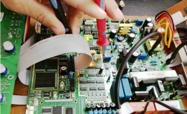
Step 8: Welding, debugging, testing, etc. If it does not meet the design requirements, please repeat the above steps.
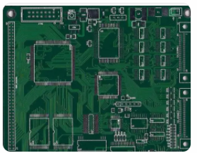
PCB design is the most important part of the above-mentioned electronic product design process, and it is also the core technology of electronic product design. In the actual circuit design, after the schematic drawing and circuit simulation are completed, the actual components in the circuit need to be finally mounted on the printed circuit board. The drawing of the schematic diagram solves the logical connection problem of the circuit, and the physical connection of the circuit board is completed with copper foil.

What is PCB?
Printed PCB refers to a board that is processed into a certain size with an insulating substrate as the basic material. There is at least one conductive pattern and all designed holes on the board (for example, component holes, mechanical mounting holes, and metallized holes, etc.) to facilitate each component Make electrical connections between:
Printed circuit boards are repeatable and predictable. All signals can be directly tested at any point along the wire, and no short circuit will be caused by the contact of the wire. The solder joints of the printed PCB can be soldered for most of them in one soldering.
Because of the above-mentioned characteristics of printing plates, they have been widely used and developed since the day they went on the market. Modern printing plates have developed in the direction of multiple layers and fine lines. Especially the SMD (Surface Mount) technology, which has been promoted since the 1980s, closely combines high-precision printed board technology and VLSI (Very Large Scale Integrated Circuit) technology, which greatly improves system installation density and system reliability.
Second, the development of printed boards.
Although printed circuit technology only developed rapidly after World War II, the origin of the concept of "printed circuit" can be traced back to the 19th century.
In the 19th century, the mass production of printed circuit boards did not have complicated electronic and electrical equipment, but a large number of passive components, such as resistors, coils, etc., were needed.
The Americans proposed the method of stamping with metal foil in 1899, and stamping the foil on the substrate to make resistors. In 1927, they proposed the method of electroplating to make inductors and capacitors.
After decades of practice, Dr. Paul Eisler in the United Kingdom put forward the concept of printed circuit boards and laid the foundation for photolithography technology.
With the emergence of electronic devices, especially transistors, the number of electronic instruments and electronic equipment has increased sharply, and has become more complicated, and the development of printed circuit boards has entered a new stage.
In the mid-1950s, with the emergence of large-scale development of high-adhesion copper clad laminates, the material foundation was laid for the mass production of printed circuit boards. In 1954, the General Electric Company of the United States adopted pattern plating: the etching method.
In the 1960s, printed boards were widely used and increasingly became an important part of electronic equipment. In addition to the extensive use of screen printing and pattern plating: etching (ie, subtractive) and other processes, an additive process is also used to increase the density of the printed lines. At present, high-level multi-layer printed circuits, flexible printed circuits, metal core printed circuits, functional printed circuits, etc. have been greatly developed.
The development of domestic printed circuit technology is relatively slow. In the mid-1950s, single-board and double-board were trial-produced. In the mid-1960s, metallized double-sided printed boards and multilayer printed boards were also trial-produced. Around 1977, electroplating-corrosion- Graphic electroplating process produces printed boards. In 1978, the additive material was trial-produced, that is, the aluminum foil-clad board, and the semi-additive method was used to manufacture the printing board. In the early 1980s, flexible printed circuits and metal core printed boards were developed.
Third, the principle of the PCB board.
Printed circuit boards generally have four uses in electronic equipment. Provide necessary mechanical support for various components in the circuit; provide electrical connection of the circuit to realize various components, such as circuit connection or electrical insulation between integrated circuits. (3) Provide the electrical characteristics of the circuit as required, such as characteristic impedance. Mark the parts installed on the board with markers to facilitate insertion, inspection and debugging.
Fourth, the types of printed boards.
The current printed circuit boards generally cover the insulating board (substrate) with copper foil, so they are also called copper clad laminates. Divided by the conductive layer of the circuit board:
(1)SingleSidedPrintBoard
Single-sided printed board refers to a printed board with conductive patterns on only one side. Its thickness is about 0.2~5.0mm. On one side of an insulating substrate coated with copper foil, a printed circuit is formed on the substrate by printing and etching. . It is suitable for the use of electronic equipment with common requirements.
There are stricter rules here: wiring rooms must not cross, and individual lines must be bypassed.
2. Double-sided printing PCB
Double-sided printed board refers to a printed board with conductive patterns on both sides. Its thickness is about 0.2~5.0mm. On both sides of an insulating substrate coated with copper foil, the printing is formed on the substrate by printing and etching. The circuit is electrically interconnected on both sides through metallized holes. The invention is suitable for electronic equipment with higher requirements, and because the wiring density of the double-sided printed board is higher, the volume of the equipment can be reduced.
3. Multilayer printed boards (Plint Bowde)
A multi-level printed board is a printed board made of staggered conductive layers and insulating material layers laminated and bonded. The conductive layers are more than two layers, and the electrical interconnection between the layers is realized through metallized holes. The multi-layer connecting lines of the printed circuit board are short and straight, which is easy to shield, but the printed circuit board has a complicated process and uses metallized holes, which is less reliable. Usually used on computer cards.
For the production of circuit boards, the more layers, the more complicated the production process, the higher the failure rate and the higher the cost, so multilayerp PCB boards can only be used for advanced circuits.