PCB design needs to be set at different points in different stages, and large grid points can be used for device layout in the layout stage;
For large devices such as ICs and non-positioning connectors, a grid point accuracy of 50 to 100 mils can be used for layout, while for small passive components such as resistors, capacitors and inductors, a grid point of 25 mils can be used for layout. The accuracy of the large grid points is conducive to the alignment of the device and the aesthetics of the layout.
What problems should be paid attention to when drawing PCB wiring
PCB layout rules:
1. Under normal circumstances, all components should be arranged on the same surface of the circuit board. Only when the top-level components are too dense, can some devices with limited height and low heat generation, such as chip resistors, chip capacitors, and chip capacitors, be installed. Chip IC, etc. are placed on the lower layer.

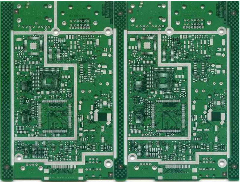
2. Under the premise of ensuring the electrical performance, the components should be placed on the grid and arranged parallel or perpendicular to each other in order to be neat and beautiful. Under normal circumstances, the components are not allowed to overlap; the arrangement of the components should be compact, and the components should be arranged on the entire layout. The distribution is uniform and dense.
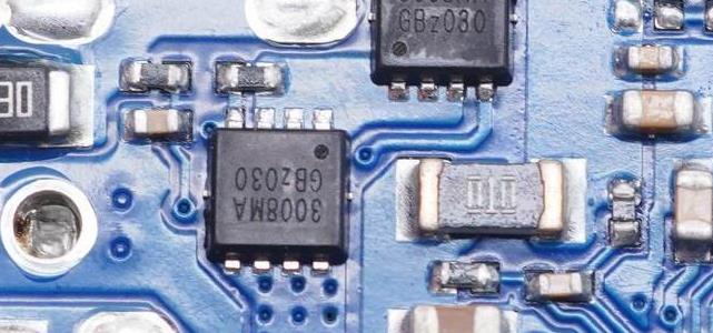
3. The minimum distance between adjacent pad patterns of different components on the circuit board should be above 1mm.
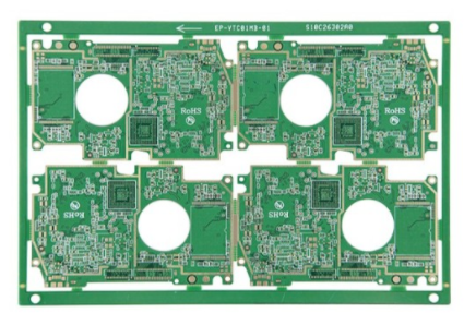
4. The distance from the edge of the circuit board is generally not less than 2MM. The best shape of the circuit board is rectangular, and the aspect ratio is 3:2 or 4:3. When the size of the circuit board is larger than 200MM by 150MM, consider what the circuit board can withstand Mechanical strength.
PCB layout skills:
In the layout design of the PCB, the units of the circuit board should be analyzed, and the layout design should be based on the starting function. When laying out all the components of the circuit, the following principles should be met:
1. Arrange the position of each functional circuit unit according to the circuit flow, so that the layout is convenient for signal circulation, and the signal is kept in the same direction as possible.
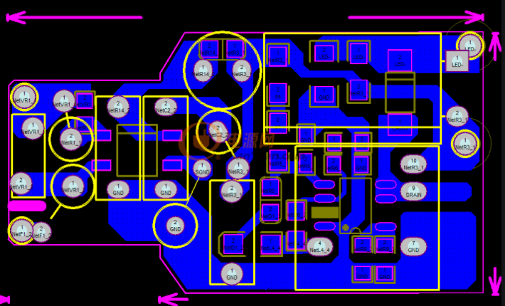
2. Take the core components of each functional unit as the center and lay out around him. The components should be uniformly, integrally and compactly arranged on the PCB to minimize and shorten the leads and connections between the components.
3. For circuits operating at high frequencies, the distribution parameters between components must be considered. In general circuits, components should be arranged in parallel as much as possible, which is not only beautiful, but also easy to install and easy to mass produce.
Special components and layout design
In the PCB, special components refer to the key components of the high-frequency part, the core components in the circuit, the components that are susceptible to interference, the components with high voltage, the components with high heat generation, and some components of the opposite sex., The location of these special components needs to be carefully analyzed, and the belt layout meets the requirements of circuit functions and production requirements. Improper placement of them may cause circuit compatibility issues, signal integrity issues, and lead to failure of PCB design.
When placing special components in the circuit board design, first consider the PCB size. When the PCB size is too large, the printed lines will be long, the impedance will increase, the anti-drying ability will decrease, and the cost will increase; if the PCB size is too small, the heat dissipation will not be good, and adjacent lines will be easily disturbed. After determining the size of the PCB, determine the swing position of the special component. Finally, according to the functional units, layout all the components of the circuit.