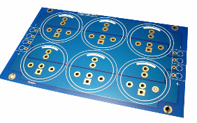
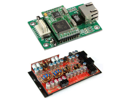
PCB width and thickness: the load flow of copper wires etched from a rigid printed circuit board. Pay attention to the height distribution of the components on the PCB and the shape and size of the PCB. For 1oz and 2oz wires, taking into account the etching method and the normal variation of copper foil thickness and the temperature difference, it is allowed to reduce the nominal value by 10% (in the load current meter), And reduce component 3 for printed circuit board components coated with a protective layer (the thickness of the substrate is less than 0.032 inches, and the thickness of the copper foil exceeds 15% ounces);
Impregnated PCB allows a 30% reduction.
PCB line spacing: The minimum line spacing must be determined to eliminate voltage breakdown or arcing between adjacent lines.
The spacing is variable and mainly depends on the following factors:
1) Peak voltage between adjacent wires.
2) Atmospheric pressure (maximum operating altitude).
3) Coating used.

4) Capacitive coupling parameters. The critical impedance components or high-frequency components are usually very close to reduce the critical phase delay.
Transformers and inductors should be isolated to prevent coupling; induction signal conductors should be placed orthogonally at right angles; components that generate any electrical noise due to magnetic field movement should be isolated or installed strictly to prevent excessive vibration.
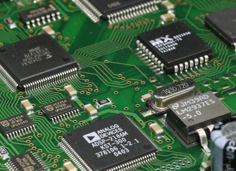
PCB copy board line graphics inspection:
1) The wires are short and straight without sacrificing functionality?
2) Does it comply with the limit of wire width? 3) Wires, wires and mounting holes, between wires and pads...
Is it necessary to keep the minimum line spacing?
4) Do you avoid parallel layout of all wires (including component leads) relatively close to each other?
5) Acute angles (90°C or less than 90°C) to avoid when drawing?
Check list of PCB copy board design items:
1) Check the rationality and correctness of the schematic diagram;
2) Check the correctness of the component package of the schematic diagram;
3) The distance between strong and weak current and the distance between isolation areas;
4) Check the corresponding schematic diagram and PCB diagram to prevent the loss of the network table;
5) Whether the packaging of the components is consistent with the physical;
6) The placement of the components is appropriate:
7) Whether the components are easy to install and disassemble;
8) Whether the temperature sensitive element is too close to the heating element;
9) The distance and direction of the transformer components can be generated is appropriate;
10) Whether the positions between the connectors correspond smoothly;
11) Easy to plug and unplug;
12) Input and output;
13) Strong current and weak current;
14) Whether digital and analog are interlaced;
15) Arrangement of upper and lower wind side components;
16) Whether the direction component is wrongly flipped instead of rotated;
17) The mounting holes of the component pins are suitable for easy insertion;
18) Check whether the empty foot of each component is normal and whether it is a leaking line;
19) Check whether there are holes in the same netlist wiring on the upper and lower layers, and whether the pads are connected through the holes to prevent disconnection and ensure the integrity of the circuit;
20) Check whether the upper and lower characters are placed correctly and reasonably. Do not place the characters on the component cover to facilitate the operation of welding or maintenance personnel;
21) The very important connection between the upper and lower lines should not only be connected to the pad that directly blocks the component, but also preferably connected to the perforated connection;
22) The arrangement of power and signal wires in the socket should ensure signal integrity and anti-interference;
23) Pay attention to the proper ratio of pads and solder holes;
24) The plug should be placed as far as possible on the edge of the PCB board for easy operation;
25) Check whether the component label is consistent with the component, and each component is placed in the same direction as possible and placed neatly;
26) In the case of not violating the design rules, the power and ground wires should be as bold as possible;
27) Under normal circumstances, the upper layer adopts a horizontal line, the lower layer adopts a vertical line, and the chamfer is not less than 90 degrees;
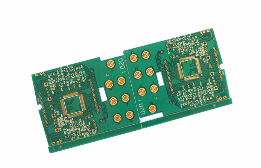
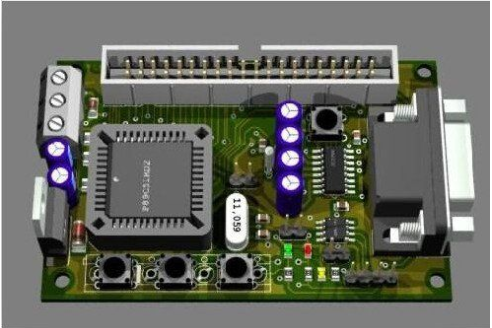
) The size and distribution of the mounting holes on the PCB copy board are suitable for minimizing the bending stress of the PCB; 2
9) Pay attention to the height distribution of the components on the PCB copy board and the shape and size of the PCB to ensure easy assembly.