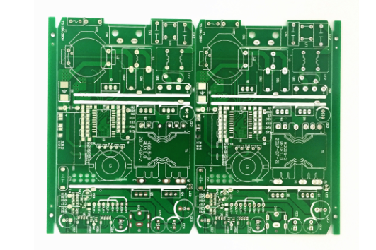
Engaged in high-frequency PCB design must have the corresponding basic theoretical knowledge, and at the same time should have a wealth of high-frequency PCB production experience. That is to say, whether it is the drawing of the schematic diagram or the design of the PCB, it should be considered from the high-frequency working environment in which it is located, in order to be able to design a more ideal PCB.
1. PCB layout design
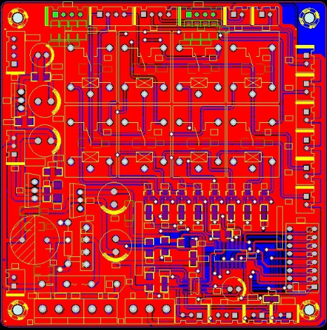
Although Protel has the function of automatic layout, it does not fully meet the working needs of high-frequency circuits. It often depends on the designer's experience and according to the specific situation. The position of some components is optimized and adjusted by manual layout, and then combined with automatic layout. Complete the overall design of the PCB. Whether the layout is reasonable or not directly affects the product life, stability, EMC (electromagnetic compatibility), etc., it must be based on the overall layout of the circuit board, the operability of the wiring, and the manufacturability of the PCB, mechanical structure, heat dissipation, EMI (electromagnetic compatibility), etc. Interference), reliability, signal integrity and other aspects are comprehensively considered.
Generally, the fixed position components related to the mechanical size are placed first, then special and larger components are placed, and finally small components are placed. At the same time, it is necessary to take into account the requirements of wiring, the placement of high-frequency components should be as compact as possible, and the wiring of signal lines can be as short as possible, so as to reduce the cross interference of signal lines.

1.1 The placement of positioning plug-ins related to mechanical dimensions
Power sockets, switches, interfaces between PCBs, indicator lights, etc. are all positioning plug-ins related to mechanical dimensions. Usually, the interface between the power supply and the PCB is placed at the edge of the PCB, and there should be a distance of 3 mm to 5 mm from the edge of the PCB; indicating that the light-emitting diodes should be placed accurately according to the needs; switches and some fine-tuning components, such as adjustable Inductance, adjustable resistance, etc. should be placed close to the edge of the PCB for easy adjustment and connection; components that need to be replaced frequently must be placed in a location with fewer components for easy replacement.
1.2 Placement of special components
High-power tubes, transformers, rectifier tubes and other heating devices generate more heat when working in high-frequency conditions, so ventilation and heat dissipation should be fully considered during layout, and these components should be placed on the PCB where air is easy to circulate. . The high-power rectifier tube and adjustment tube should be equipped with a radiator and kept away from the transformer. Heat-resistant components such as electrolytic capacitors should also be kept away from heating devices, otherwise the electrolyte will be dried, causing its resistance to increase, performance degradation, and affecting the stability of the circuit
Components that are prone to failure, such as adjustment tubes, electrolytic capacitors, relays, etc., should be placed in consideration of easy maintenance. For test points that often need to be measured, care should be taken to ensure that the test rods can be easily touched when arranging components.
Since a 50 Hz leakage magnetic field is generated inside the power supply device, when it is cross-connected with some parts of the low-frequency amplifier, it will interfere with the low-frequency amplifier. Therefore, they must be isolated or shielded. It is best to arrange each level of the amplifier in a straight line according to the schematic diagram. The advantage of this arrangement is that the ground current of each level is closed and flows at this level, and does not affect the operation of other circuits. The input stage and output stage should be as far away as possible to reduce the parasitic coupling interference between them.
Considering the signal transfer relationship between the functional circuits of each unit, the low-frequency circuit should be separated from the high-frequency circuit, and the analog circuit and the digital circuit should be separated. The integrated circuit should be placed in the center of the PCB to facilitate the wiring connection of each pin with other devices.
Devices such as inductors and transformers have magnetic coupling and should be placed orthogonally to each other to reduce magnetic coupling. In addition, they all have a strong magnetic field, and there should be a suitably large space or magnetic shielding around them to reduce the impact on other circuits.
Appropriate high-frequency decoupling capacitors should be configured on the key parts of the PCB. For example, an electrolytic capacitor of 10 μF ~ 100 μF should be connected to the input end of the PCB power supply, and a ceramic of about 0.01 pF should be connected near the power supply pin of the integrated circuit. Chip capacitors. Some circuits must be equipped with appropriate high-frequency or low-frequency chokes to reduce the impact between high- and low-frequency circuits. This should be considered when designing and drawing the schematic, otherwise it will also affect the performance of the circuit.
The spacing between the components should be appropriate, and the spacing should take into account whether there is a possibility of breakdown or ignition between them.
For amplifiers containing push-pull circuits and bridge circuits, attention should be paid to the symmetry of the electrical parameters of the components and the symmetry of the structure during the layout, so that the distribution parameters of the symmetrical components are as consistent as possible.
After the manual layout of the main components is completed, the method of component locking should be adopted so that these components will not move during the automatic layout. That is, execute the Edit change command or select Locked in the Properties of the component to lock it and no longer move it.
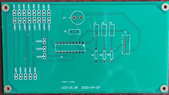
1.3 Placement of common components
For common components, such as resistors, capacitors, etc., should be considered from several aspects such as the neat arrangement of the components, the size of the occupied space, the operability of the wiring and the convenience of welding, and the automatic layout method can be adopted.
PCB routing is the overall requirement for high-frequency PCB design based on a reasonable layout. Wiring includes automatic wiring and manual wiring. Generally, regardless of the number of key signal lines, manually route these signal lines first. After the wiring is completed, carefully check the wiring of these signal lines, fix them after passing the inspection, and then automatically route other wiring. That is, a combination of manual and automatic wiring is used to complete the wiring of the PCB.