I wrote these because I saw that some netizens were a little confused about these aspects. At the same time, when discussing with some people in PCBA/designer, I felt that these matters were not fully considered, so I summarized them here for reference.
If you have any questions, please ask.
There are the following matters:
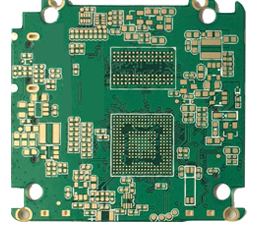
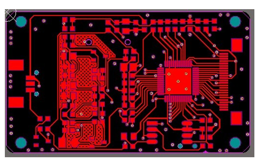
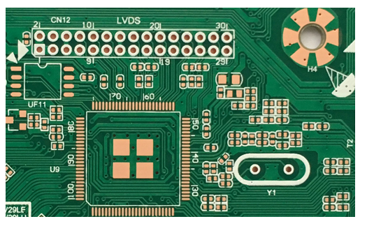
1. What is the tolerance of your finished BGA pad?
For different tolerance requirements, PCB manufacturers generally have different processes to compensate/increase the value of the BGA pad. At the same time, because the PCB manufacturer's process has a minimum spacing (pitch) requirement, this will limit your BGA pitch setting;
If the tolerance is large and the spacing is small, then the finished BGA pad will be biased towards the lower limit of the tolerance, which is not conducive to the welding of BGA;
If the tolerance is small and the spacing (spacing) is also small, the process compensation value of the PCB manufacturer cannot be satisfied because there is not enough spacing, or the size of the BGA pad is seriously lowered, or it exceeds the tolerance requirements (of course, there will be a certain percentage of ). Or few PCB manufacturers can accept this design. Of course, the delivery date and the stability of tea quality are all problems.
2. How much does your manufacturer have to compensate to meet your tolerance requirements for finished products?
See item 1.

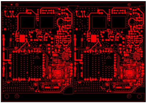
3. How much spacing does your manufacturer need to ensure that there is no BGA pad on the solder mask?
This is the space that must be reserved in addition under the premise of item 1.
This is also one of the factors that affect your BGA pitch settings.
4. Is it required to have a solder mask covering between the BGA pads?
This is what PCB manufacturers call the "green oil bridge" problem;
If so, then this is the third factor to reserve spacing;
This is also one of the factors that affect your BGA pitch settings.
5. How wide is the spacing required by your manufacturer to ensure that there is solder mask on the board?
See item 4.
If it is too narrow, the "green oil bridge" will fall.
If there is no "green oil bridge", some PCB installation manufacturers may have soldering problems in their processes - the amount of effective solder paste is insufficient.
6. Do you want to route between BGA pads?
If you want to wire, then the width of the line, the number of lines, the distance between the lines, and the distance between the line and the area that is not covered with green oil are all factors to be considered when setting the BGA pitch;
These include items 7, 8, and 9.
7. If wiring, what is the tolerance of the finished wire? How much does your manufacturer have to compensate to meet your requirements?
Similar to item 1.
8. If wiring, how much spacing does your manufacturer need to ensure that the solder mask can completely cover the wires?
This is because there are tool alignment deviations in the PCB manufacturer's process. That is, when the operator aligns the green oil imaging tool with the PCB board, 100% alignment cannot be guaranteed. There are both reasons for the proficiency of the operator and the dimensional stability of the PCB board.
9. If the wiring is more than one line, your manufacturer must maintain the spacing between the lines after the line compensation (spacing) before etching (etching)
Done successfully?
This is a comprehensive consideration of items 6, 7, and 8.