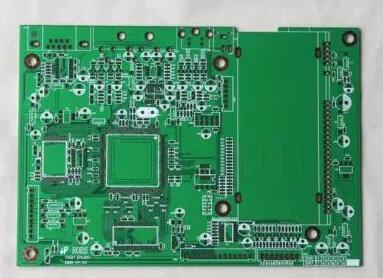
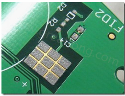
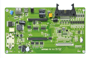
There are many ways to design jigsaw puzzles, and it is sometimes difficult to determine which jigsaw method and the number of jigsaw puzzles to use during the trial production of new products. PCB design engineers give priority to meeting the structural requirements of the product during the design according to product characteristics (such as product structure limitation, peripheral interface height limitation, position limitation, etc.), followed by feedback of sheet utilization and production during PCB manufacturing and SMT processing. The question of efficiency. After the PCB board is selected in the production process, the thermal expansion after encountering different geometric dimensions and PCB boarding methods directly affects the reliability and performance of the product, which increases the processing difficulty and manufacturing cost of SMT production. Combining the experience summaries of SMT process engineers for many years, the use of jigsaw method to improve the efficiency of SMT production line, there are the following aspects to share with you:

· In the SMT production line, in order to increase the utilization rate of the production line, there are two common ways of splicing AAAA or AB. We can't directly ask which one is better? This should be considered from the complexity of the product process, the balance rate of the placement cycle of the production line machine after the panel is assembled, and the problem of parts drop after the second remelting of the bulky component, and so on.
· The positive and negative design (AABB) has the advantage of making SMT production line equipment configuration and process simple and easy. A stencil, a set of patch procedures, spi/AOI inspection procedures, and reflow soldering furnace temperature curve optimization once, etc., to increase the speed of SMT rapid line change and complete the first piece verification at one time, and PCBA finished products can be produced in a very short time Give out to the next process function test.
·The disadvantage of the positive and negative design (AABB) is that if the product BOT surface and the TOP surface have a large difference in component layout (the main chip is larger, the component layout density is higher, and the through-hole reflow component feet exceed the board surface. Etc.) will lead to poor and unstable solder paste printing at fine pitch positions, risk of dropping parts for components with large volume and weight during the second pass. In mass production, not only the efficiency improvement problem is not solved, but also the processing difficulty and quality are caused. The problem, this is also a test of engineers' online technical research capabilities.
· Adopt (AAA/BBB) non-positive and negative design, which is more suitable for the recommendation of most factories. The production line is easy to deploy and the equipment resources are rationally arranged. The production process is stable, and it is easy to improve the efficiency of the production line. When designing the PCB, engineers must consider the rationality of the layout of the overall main chip components, larger heat dissipation components, and peripheral interface components. The processing plant only needs to reasonably arrange the production line to produce the BOT surface (less component surface) and then the TOP surface (multiple component surface). ), the process engineering is easier to deal with when the quality is abnormal during the processing.