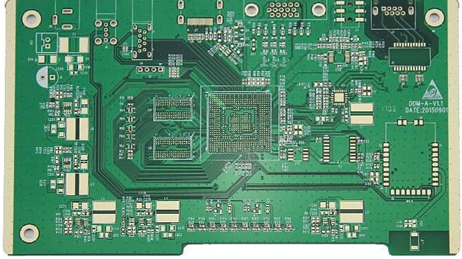
Layout, that is, on the basis of comprehensive consideration of signal quality, EMC, thermal design, DFM, DFT, structure, safety regulations, etc., the components are placed on the board reasonably. In high-speed PCB design, a reasonable layout is the first step to a successful PCB design.
What is the PCB design layout idea
Layout ideas
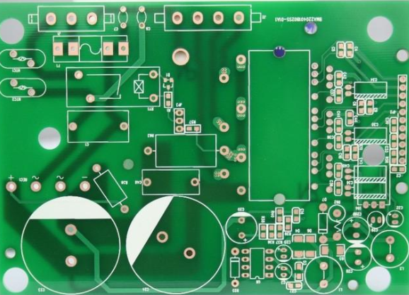
In the PCB layout process, the first consideration is the size of the PCB. Secondly, it is necessary to consider the devices and areas with structural positioning requirements, such as whether the height is limited, the width is limited, and the area of punching and slotting. Then, pre-layout each circuit module according to the circuit signal and power flow direction, and finally carry out the layout work of all components according to the design principles of each circuit module.

Basic principles of layout
1. Communicate with relevant personnel to meet special requirements in terms of structure, SI, DFM, DFT, and EMC.
2. According to the structural element diagram, place the components that need to be positioned such as connectors, mounting holes, indicator lights, and give these components non-movable attributes, and carry out dimensions.
3. According to the structural element diagrams and the special requirements of certain devices, set up no-wiring area and no-layout area.
4. Comprehensive consideration of PCB performance and processing efficiency to select the process flow (preferably single-sided SMT; single-sided SMT + plug-in; double-sided SMT; double-sided SMT + plug-in), and layout according to the characteristics of different processing technology.
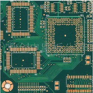
5. Refer to the results of the pre-layout when layout, according to the layout principle of "big first, then small, first difficult then easy".
6. The layout should meet the following requirements as far as possible: the total wiring is as short as possible, and the key signal line is the shortest; high voltage and large current signals are completely separated from weak signals of low voltage and small current signals; analog signals and digital signals are separated; high frequency The signal is separated from the low-frequency signal; the distance between the high-frequency components should be sufficient. Under the premise of meeting the requirements of simulation and timing analysis, local adjustments are made.
7. As far as possible, the same circuit part adopts a symmetrical modular layout.
8. The recommended grid for layout setting is 50mil, and for IC device layout, the recommended grid is 25 25 25 25 mil. When the layout density is high, the grid setting of small surface mount devices is recommended to be no less than 5mil.
The layout principle of special components
1. Minimize the length of wiring between FM components as much as possible. The components that are susceptible to interference should not be too close to each other, try to reduce their distribution parameters and mutual electromagnetic interference.
2. For devices and wires that may have a higher potential difference, the distance between them should be increased to prevent accidental short circuits. Devices with strong electricity should be placed in places where the human body is not easy to reach.
3. Components weighing more than 15g should be fixed with brackets and then welded. For large and heavy components that generate a lot of heat, it is not suitable to be installed on the PCB. The heat dissipation problem should be considered when installed on the housing of the whole machine, and the heat-sensitive components should be far away from the heating components.
4. The layout of adjustable components such as potentiometers, adjustable inductance coils, variable capacitors, micro switches, etc. should consider the structural requirements of the whole machine, such as height limit, hole size, center coordinates, etc.
5. Reserve the position occupied by the PCB positioning hole and the fixed bracket.
Check after layout
In PCB design, a reasonable layout is the first step to a successful PCB design. After the layout is completed, engineers need to strictly check the following:
1. PCB size mark, whether the device layout is consistent with the structure drawing, and whether it meets the PCB manufacturing process requirements, such as minimum aperture and minimum line width.
2. Whether the components interfere with each other in two-dimensional and three-dimensional space, and whether they interfere with the structural shell.
3. Whether all the components have been placed.
4. Whether the components that need to be frequently plugged or replaced are easy to plug and replace.
5. Whether there is a proper distance between the thermal device and the heating element.
6. Whether it is convenient to adjust the adjustable device and press the button.
7. Whether the position where the radiator is installed is unobstructed.
8. Whether the signal flow direction is smooth and the interconnection is the shortest.
9. Is there any consideration for line interference?
10. Whether the plug and socket contradict the mechanical design.