The aluminum base plate is a new type of heat sink metal plate. It is also different from the traditional heat dissipation metal plate. The inherent characteristics of the aluminum base plate can minimize the thermal conductivity, so that more heat can be discharged to the greatest extent. The cooling effect. The aluminum substrate is mainly composed of three parts, namely the circuit layer, the insulating layer and the metal layer, and a double-sided board is used in some high-end aluminum substrate designs. This double-sided board is almost not used on the traditional radiator metal plate. Because most traditional metal plates use multi-layer boards, but the disadvantage of multi-layer boards is that the heat dissipation effect cannot be maximized and cannot meet the heat dissipation needs of users

As a new type of heat-conducting metal plate, aluminum substrate has been widely used now. In home computers, car audios and our most popular LED lights nowadays, their radiator metal plates are all aluminum substrates. In many areas where aluminum substrates are used, it must be attributed to its own advantages. So what are its high-quality characteristics? The editor has compiled the data as follows:
The surface of the aluminum substrate adopts a special technology-surface mount. Through this technology, it can treat the heat generated by the product to the maximum extent during the heat dissipation process or in the PCB circuit design to achieve the best heat dissipation. Effect.
A major feature of the aluminum substrate is that it can minimize the product temperature while ensuring that the product's use efficiency will not be reduced, because if the product use efficiency is reduced, the gain will not be worth the loss. In addition, the aluminum substrate is to a certain extent It can extend the service life of the product.
The volume of the aluminum substrate is small, so its cost price and occupied space area are relatively small.
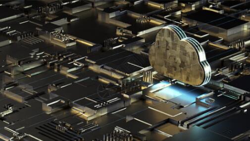
In recent years, as the functions of various portable consumer electronic products continue to increase, PCB boards have become smaller and smaller, and test boards must require PCB boards that carry electronic components to be lighter, thinner, shorter, and smaller. Among the test boards, High Density Interconnection (HDI) is used more and more widely. Cell phone boards, tablet computers, semiconductor packaging substrates, car satellite navigation systems and other fields require high-density interconnection PCB boards to support. The demand for high-density interconnect PCB boards is increasing, and the requirements for the uniformity of the board surface copper are also increasing. The increase in process difficulty also increases the difficulty of production. A mistake in one link will cause major losses. Therefore, the test board is manufactured before production to reduce the risk of the entire production process and increase the board yield rate.

The parameters of the copper wires of high-density interconnection PCB boards are one of the criteria for evaluating the pass rate of high-density interconnection PCB boards. Any defect in the copper wires will evolve into poor circuits, and even lead to lower yields, higher costs, and lower production efficiency. A series of disadvantages such as reduction and extension of product production cycle, and the traditional template structure for testing the pass rate of copper wire parameters of high-density interconnection circuit boards is complicated and high in cost.
The CB test board is provided with a plurality of test pattern units, and each test pattern unit includes a first test line, a second test line, a third test line, and a fourth test line. Since the extension directions of the first test line, the second test line, the third test line, and the fourth test line are different from each other and do not overlap each other, and the first test line, the second test line, the third test line, and the The line widths of the four test lines are all equal. By testing the line widths of the test lines in different extension directions, it can be judged whether the PCB board prepared by the same process is qualified. The test structure is simple and the cost is low., And easy to operate.