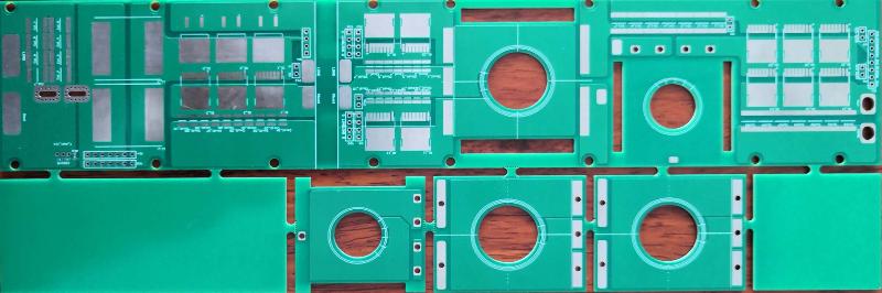
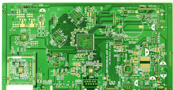
Modern PCBA electronic assembly is a relatively complicated process. In the production process, PCB circuit board defects are caused due to factors in the PCB substrate and PCB circuit board processing. Next, the editor will introduce several common PCB defects and their causes.
In the PCB manufacturing process, common PCB circuit board defects include: white spots, micro-cracks, blistering, delamination, wet weaving, exposed fabric, halo and solder mask defects.
1. Vitiligo
At the interweaving point of the glass fiber on the surface of the sheet, the resin is separated from the fiber, and white spots or "cross patterns" appear under the surface of the substrate.
reason:
(1) When the board is subjected to improper mechanical external force impact, the local resin and glass fiber are separated into white spots.
(2) Part of the board material is penetrated by fluorine-containing chemicals and etches the weave points of the glass fiber cloth, forming regular white spots (it can be seen as a square when it is more serious).
(3) Improper thermal stress on the board can also cause white spots and white spots.
2. Micro cracks
A continuous white spot or "cross pattern" that occurs inside the laminated substrate can be defined as a microcrack.
Reason: Mainly affected by mechanical stress, microcracks are generated inside the laminated substrate.
3. Foaming
The imagination of local separation caused by local expansion between the layers of the substrate or between the substrate and the conductive foil, between the substrate and the protective coating.
reason:
(1) Panel surface pollution (oxidation, oil stains, glue marks, other alkaline pollution)
(2) Insufficient post-curing time, most of which manifested as bubbling and oil loss on both sides of a corner, which was discovered after tin spraying.
(3) The tin stripping is not clean, and there is a thin layer of tin on the board surface. After the tin is sprayed, the tin on the board surface will be melted at a high temperature and the ink will be lifted up to form a bubble.
(4) The ink is printed before the water vapor in the hole is dried. After spraying tin, it will form ring-shaped bubbles on the edge of the hole where the water is stored.
(5) Imagine that there is water vapor in the PCB during the soldering process of the PCB circuit board, and it is easy to generate bubbles during reflow soldering.

4. Layering
Imagine the separation between the substrate layers, the insulating substrate and any layer in the conductive or multilayer board.
reason:
(1) Laminating parameters are not set as required by the specification
(2) Inadequate cleaning and debris on the board surface, resulting in delamination after welding.
5. Wet fabric
The braided fabric fibers that are completely covered by resin and are not broken in the base material present a woven pattern on the surface.
6, exposed fabric
A phenomenon in which braided fibers are exposed on the surface of the substrate that are not completely covered by resin or are not broken.
7, halo
Destruction or delamination on the surface of the substrate or under the surface is usually manifested as a white area around the hole or other processed parts.
reason:
(1) The machine table or the bakelite board is uneven, and there is a gap between the board and the bakelite board.
(2) The board is warped and deformed, and there are gaps between the boards
(3) Milling cutter wear
(4) The inspector is not clear about the missed inspection of the second-diamond halo standard.
8. Solder mask defects
Solder mask is a heat-resistant coating material, and solder mask defects can easily lead to the deposition of solder in the non-soldering area during PCB soldering.
reason:
(1) The spacing or air gap around the pad feature is too large
(2) After the solder mask is printed, the baking time and temperature are not enough, causing the solder mask to not completely solidify. After the high temperature impact of the furnace, the solder mask layered bubbles.
These PCB defects are an important factor affecting the defect rate of electronic products. By understanding these defects and their causes, the process can be improved during the electronic assembly process and the product yield rate can be improved.