1. Introduction to noun interpretation
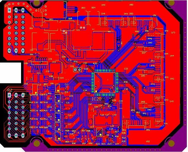
Printed circuit--on the surface of insulating material, a conductive pattern that provides electrical connections between components (including shielding components).
Printed circuit-On the surface of the insulating material, according to a predetermined design, a printed circuit, a printed element, or a circuit composed of the two are made by a printing method, which is called a printed circuit.
Printed circuit/circuit board-a collective term for insulating boards that have completed printed circuits or printed circuit processing.
low-density printed circuit boards-mass production of printed circuit boards, a wire is laid between the two disks at the intersection of the 2.54 mm standard coordinate grid, and the wire width is greater than 0.3 mm (12/12 mil).
Medium-density printed circuit board-mass production of printed circuit boards, two wires are laid between the two disks at the intersection of the 2.54 mm standard coordinate grid, and the wire width is about 0.2 mm (8/8 mil).
High-density printed circuit board-mass production of printed circuit boards, three wires are laid between the two disks at the intersection of the 2.54 mm standard coordinate grid, and the wire width is 0.1~0.15 mm (4-6/4-6mil) ).
2. How many types of printed circuits are divided into substrates and conductive patterns used?

--According to the substrate used: rigid, flexible, rigid-flexible;
--According to the conductive pattern: single-sided, double-sided, multi-layer.
3. Briefly describe the role of the printed circuit and the characteristics of the printed circuit industry?
--First of all, it provides mechanical support for PCB fixing and assembly for transistors, integrated circuits, resistors, capacitors, inductors and other components.
Secondly, it realizes the wiring and electrical connection and electrical insulation between transistors, integrated circuits, resistors, capacitors, inductors and other elements to meet their electrical characteristics.
Finally, it provides identification characters and graphics for the inspection and maintenance of components in the PCB electronic assembly process, and provides solder mask graphics for wave soldering.
--High technology, high investment, high risk, high profit.
4. What are the main two methods for the classification of printed circuit manufacturing processes? What are the advantages of each?
--Additive method: avoid a large amount of copper etching and reduce the cost. The production process is simplified and the production efficiency is improved. Able to achieve flush wires and flush surfaces. Improve the reliability of metallized holes.
--Subtractive method: The process is mature, stable and reliable.
5. How many types are the additive processes of printed circuit manufacturing divided into? Write down the process separately?
--Full additive method: drilling, imaging, viscosity increasing treatment (negative phase), electroless copper plating, resist removal.
--Semi-additive method: drilling, catalytic treatment and viscosity increasing treatment, electroless copper plating, imaging (electroplating resist), pattern copper electroplating (negative phase), resist removal, differential etching.
--Partial addition method: imaging (anti-etching), etching copper (normal phase), removing the resist layer, coating the entire plate with electroplating resist, drilling, electroless copper plating in the hole, and removing electroplating resist.
6. How many types are printed circuits in the subtractive process divided into?
Write down the process flow of PCB full-board electroplating and pattern electroplating.
--Non-perforated plated printed circuit boards, perforated plated printed circuit boards, perforated plated printed circuit boards and surface mounted printed circuit boards.
--PCB full-board plating (masking method): double-sided copper clad plate blanking, drilling, hole metallization, full-board plating thickening, surface treatment, photo-masking dry film, making positive phase conductor patterns, etching, Film removal, plug electroplating, shape processing, inspection, printing solder mask, hot air leveling, screen printing marking symbols, finished products.
--PCB graphic electroplating (bare copper clad solder mask): double-sided copper clad plate blanking, punching positioning holes, CNC drilling, inspection, deburring, electroless thin copper plating, thin copper electroplating, inspection, brushing, filming ( (Or screen printing), exposure and development (or curing), inspection and repair, pattern copper plating, pattern tin-lead alloy plating, film removal (or removal of printing materials), inspection and repair, etching, lead and tin removal, on-off test, cleaning, Solder mask graphics, plug nickel/gold plating, plug tape, hot air leveling, cleaning, screen printing marking symbols, shape processing, cleaning and drying, inspection, packaging, finished products.
7. Which types of electroplating technology can be divided into?
--Conventional hole plating technology, direct plating technology, conductive adhesive technology.
8. What are the main features of flexible printed circuit boards? What are the base materials?
--It can be bent and folded to reduce the volume; light weight, good wiring consistency, and high reliability.
9. Briefly describe the main features and uses of rigid-flexible printed circuit boards?
--The rigid and flexible parts are connected into one body, the connector is omitted, the connection is reliable, the weight is reduced, and the assembly is miniaturized. PCB is mainly used for medical electronic equipment, computers and peripherals, communication equipment, aerospace equipment and national defense and military equipment.
10. Briefly describe the characteristics of conductive offset printed circuit boards?
--The processing technology is simple, the production efficiency is high, the cost is low, and the waste water is small.
11. What is a multi-wiring printed circuit board?
--The printed circuit board made by laying metal wires directly on the insulating substrate in layers.
12. What is a metal-based printed circuit board? What are its main features?
-the general term for metal base printed circuit boards and metal core printed circuit boards.
13. What is a single-sided multilayer printed circuit board? What are its main features?
--Manufacturing multilayer circuit boards on single-sided printed circuit boards. PCB features: not only can inhibit the internal electromagnetic waves from radiating outwards, but also prevent the interference of external electromagnetic waves to it. It does not require hole metalization, low cost, light weight, and thinner.
14. Briefly describe the definition and manufacturing of multilayer multilayer printed circuits?
--Insulating layers and conductive layers are alternately made on the inner layer of the completed multilayer board in a laminated manner, and the layers are freely connected by blind holes to make a printed circuit board with high-density multilayer wiring.