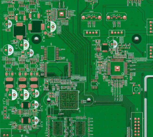
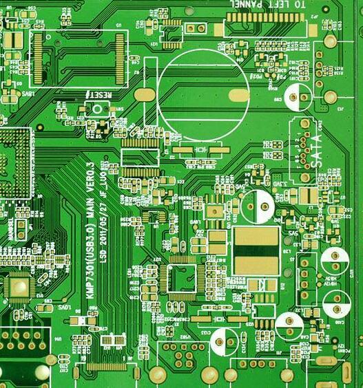
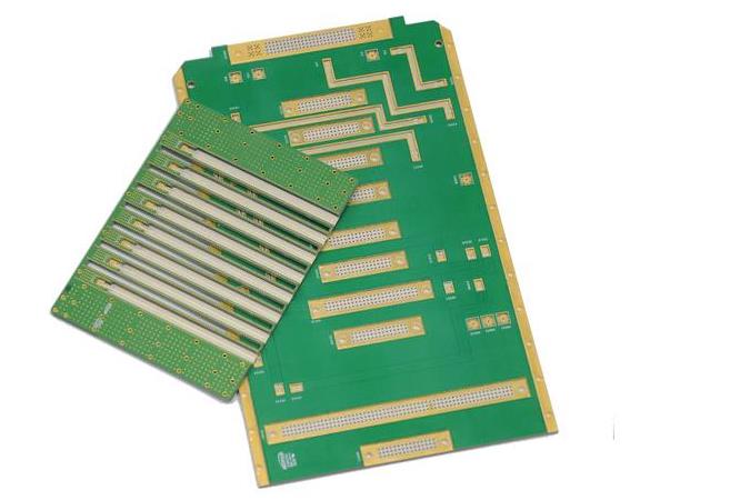
PCB company products have a [micro-short circuit phenomenon in the inner layer of the circuit board]. After investigation, it was found to be CAF (Conductive Anodic Filament), which is called "conductive anode filament" or "anode glass fiber filament leakage phenomenon" in Chinese. But in literal translation, few people can figure out what this stuff is, right? CAF is actually the phenomenon of micro-short circuit in the inner layer of the circuit board or the solder resist green paint layer.
Because this problem has been lingering in the heart of Shenzhen Honglijie, with the deduction of time, some courses on PCB manufacturing have been added, and after discussing with more PCB manufacturers, they have summed up some information about CAF. I put my experience here for your reference.
The formation principle of CAF
Refer to the top diagram to illustrate the process of CAF formation. CAF refers to the DC voltage applied to the printed circuit board and placed in a high-humidity environment. Line), Hole to Hole or Hole to Line, the copper metal in the high potential anode will be oxidized to Cu+ or Cu++ ions first, and follow the glass fiber yarn of the existing bad channel The beam slowly migrates and grows toward the cathode, and the electrons from the cathode also move toward the anode. During the journey, copper ions encounter electrons and will be reduced to copper metal, and gradually spread from the anode to the cathode to form a copper film, so it is also called " Copper migration".

Many people encounter CAF for the first time and will always be troubled by its repeated behavior, because once CAF has completed the path of conduction, it will be burned by high-resistance Joule heat from time to time, so use an electric meter to separate When measuring CAF, you will find the phenomenon of ups and downs, and the measured value will always drift. Before the specific conditions disappear, the CAF scene will appear repeatedly in the same position.
To sum up, to form a CAF defect, the following five failure conditions must be met at the same time. That is to say, there must be an absolute right time and place to produce CAF. Therefore, accidents are not accidental, but are formed by a series of errors. of:
1. Water vapor (unavoidable in atmospheric environment)
2. Electrolyte (seems difficult to remove)
3. Exposure of copper (copper foil is used as the substrate in the circuit board, so it cannot be avoided)
4. Bias voltage (the circuit design is inevitable, so it cannot be avoided)
5. Channel (it seems that this parameter can only be improved)
Metal ions undergo electrochemical migration (ECM, Electro Chemical Migration) reactions in non-metallic media under the action of an electric field, thereby forming a conductive channel between the anode and cathode of the circuit and causing the circuit to short circuit
Anode: Cu - Cu2++2e– (Copper dissolved at anode)
H2O - H++OH-
Cathode: 2H++2e– - H2
Cu2++2OH-- - Cu(OH)2
Cu(OH)2 - CuO+H2O
CuO+H2O - Cu(OH)2 - Cu2++2OH--
Cu2++2e-- - Cu (Copper deposited at cathode)
It is generally believed that ion migration is divided into two stages: In the first stage, the resin and the reinforcing material are chemically hydrolyzed by the silane coupling agent of the reinforcing material under the action of moisture, that is, forming on the epoxy resin/reinforcing material along the reinforcing material The leakage path of CAF is a reversible reaction at this stage; in the second stage, under the action of voltage or bias, the copper salt undergoes an electrochemical reaction, depositing conductive channels between circuit patterns, causing short circuits between circuits. This stage is an irreversible reaction.
How can we prevent or solve the occurrence of CAF?
To solve or prevent the occurrence of CAF, in fact, we can start from the above five necessary conditions. As long as any one of these conditions is eliminated, it can be prevented from occurring.
1. Improve the ability of circuit board materials in Anti-CAF
The selection of circuit board materials is actually very important to prevent the occurrence of CAF, but usually you get what you pay for. Generally, substrates with high CAF protection capabilities require special ordering. The bottom is to use circuit board substrates to prevent CAF. Suggestions:
Reduce the content of impure ions in the material.
The glass fiber cloth is fully impregnated with resin to bond well.
When the PCB substrate is made, multiple bundles of glass fiber bundles are woven into a cloth, and then they are introduced into the resin tank to soak, and then gradually pull up or pull out the resin-soaked glass fiber cloth, the purpose is to allow the resin to fill the glass fiber bundles Among the gaps, if the parameters at this stage are not set well, gaps are easily formed in the glass fiber bundles, so that CAF has gaps to take advantage of.
Use low hygroscopic resin. Related reading articles: Introduction to the structure and function of PCB board
2. PCB layout Design avoids bias voltage and hole spacing
The circuit board's through holes, circuit size and location, and stacking structure design will also have an absolute impact on CAF, because almost all requirements come from design. As products become smaller and smaller, the density of circuit boards is getting higher and higher, but the PCB process capability has its limits. When the distance between adjacent lines with DC bias voltage (bias voltage) is smaller, the probability of CAF occurrence is also Higher and higher, basically the higher the bias voltage or the smaller the distance, the higher the probability of CAF.
According to the information provided by the current circuit board manufacturers, the following are the PCB size design values recommended by most circuit board manufacturers for CAF protection:
Distance from hole to hole edge (minimum): 0.4mm
Hole to line distance (minimum) (Drill to Metal): 12mil (0.3mm)
Aperture recommendation: 0.3mm
In addition, according to actual experience, it is found that the gaps of CAF are almost all along the same glass fiber bundle, so if the arrangement of through holes or pads can be arranged at a 45-degree angle, it will help to reduce the CAF. Incidence rate.
CAF improvement measures-design. According to actual experience, it is found that the gaps of CAF are almost all along the same glass fiber bundle, so if the arrangement of through holes or pads can be arranged at a 45-degree angle, it will help reduce the incidence of CAF. .
3. Wicking control in PCB manufacturing process
High temperature will be generated during mechanical drilling or laser burning of PCB, which will melt and form slag when it exceeds the Tg point of resin. This slag will adhere to the inner copper edge and the hole wall area. In the subsequent copper plating, the contact is poor. Therefore, the de-smear operation must be carried out before the copper plating. Various glue residues swell and relax to facilitate the subsequent smooth penetration and bite erosion of Mn+7. However, the de-smear operation will also cause a certain bite corrosion to the through hole and possible wicking (wicking). Some circuit board manufacturers will increase the temperature of the fluffing groove in order to speed up the fluffing operation, resulting in fluffing agent Excessive slackening of the interface causes subsequent copper migration.
IPC-A-600 stipulates that the acceptance standard for Wicking is as follows:
Class 1, copper infiltration shall not exceed 125µm (4.291 mil)
Class 2, copper infiltration should not exceed 100µm (3.937 mil)
Class 3, copper penetration should not exceed 80µm (3.15 mil)
Wicking control in PCB manufacturing process
It’s just that with the advancement of technology, 0.1mm (100µm) copper infiltration does not seem to meet the actual needs. From the 0.4mm hole to the edge of the hole, deducting the size of the copper infiltration, the distance is only 0.4-0.1-0.1. = 0.2mm. Based on the current process capability of circuit board manufacturers, it should be possible to control the copper penetration below 50µm (2mil). In contrast, the distance from the hole to the hole of the Layout circuit board in the system factory has also been reduced to 100µm (4mil), which is really a big test for the prevention and control of CAF.
In addition, during the mechanical drilling of PCB, if the feed speed is too fast, or the milling cutter exceeds the service life, it is easy to tear the glass fiber and create a gap due to the external force of the milling cutter.
4. Waterproof and moisture control during PCB processing
In the PCB Assembly operation, solder paste printing, part attachment, high temperature reflow, etc. may leave some contaminants on the circuit board. These contaminants may include solder, glue, dust, and condensation. Such substances that are prone to electrolysis may cause electrochemical migration. Sealants can be used to seal the junctions that may create voids and form CAFs to prevent the infiltration of moisture.