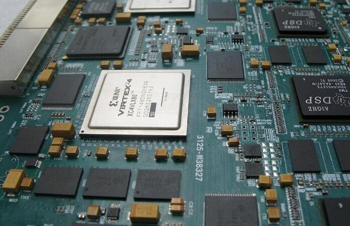
After having the basis of PCB automatic wiring, we can easily make manual wiring adjustments. The following will explain the shortcomings of Protel DXP's automatic wiring, and make wiring adjustments based on the Mypcb.PCBDov circuit board file we have done.
1. In Protel DXP, manually modify the wiring with too many turns
Protel DXP’s automatic routing often has too many corners due to the algorithm, which tends to make the view look rather annoying. After manual adjustment, this phenomenon can be greatly improved. This adjustment will involve the mutual positional relationship of multiple wires, and even re-plan the overall layout.
In the automatically routed board in the Mypcb.PCBDoc example, it is easy to find a line with too many corners. It can be seen from the upper left corner that the corners of the wiring are too cumbersome. Especially the wires of the NetU6_15 network and the wires of the -12 network, there are many wiring corners and they also restrict each other. After detailed analysis, it is determined that there will be a better wiring method after the wiring adjustment. The wiring adjustment plan is introduced in detail below:
Let's take a closer look at the automatic routing of the wires of the -12 network, select the filter condition as network in the filter toolbar, and select the -12 network in the drop-down menu to filter the -12 network.

It can be seen that the -12 network is routed from the bottom through a via to pass from the bottom layer to the top layer. The wiring at the bottom layer is straight and the automatic wiring is good, but a small piece of wire at the top layer is bent and has too many corners. Moreover, due to the unreasonable arrangement of this section of wire, it also caused too many wire routing corners of the network NetU6_15, taking unnecessary paths.
Therefore, we set up a plan to increase the position of the vias so that the wires on the top layer of the -12 network can be connected from above the GND pad of J2 to the -12 solder joint of U11. The steps are as follows, first raise the position of the via. Select the TopLayer layer, then delete the wire on the right side of the via, and redraw the wire from the via to the -12 pad of the U11 component to get the wiring scheme.
The wire of the network NetU6_15 is such a problem. It can be routed straight, but the automatically routed wire has many turns in this way. In the same way, we also filter out the wires of the network NetU6_15. Similarly, in the Toplayer layer, we delete all inflection points and re-plan the wiring. The wiring after adjustment has been well improved, and the comparison of the network wiring before and after the change.
It can be seen that after the PCB wiring is adjusted, the layout of the wires is more reasonable and beautiful, and the wires will not be squeezed into a ball like before the adjustment, which is not conducive to current transmission and unsightly.
2. Manually modify the wiring in Protel DXP to adjust the density of wiring
After automatic routing, it is often found that only a part of the PCB board is wired. This part of the area has a high wiring density, but there is still a lot of space for wiring in some areas. In this case, we can follow the following steps to deal with it:
1) First reduce the range of the circuit board appropriately, and redo the layout and routing. Stop the redesign of the PCB area when the blank area is greatly reduced.
2) Arrange the wires in the sparsely-wiring area on the circuit board properly and tightly, leaving room for the densely-wiring area for adjustment.
3) Adjust the area with high wiring density and transfer it to the area with sparse wiring.
The wiring adjustment for this kind of problem is very troublesome. Try to adjust the layout of the components and the wiring strategy during automatic wiring to avoid uneven wiring. Even if this kind of uneven wiring occurs, don't worry, just modify it patiently.
3. In Protel DXP, manually modify the wiring and move the wiring that is seriously unreasonable.
Some wires will affect the wiring of the wires next to them due to their location. At this time, we need to adjust the position of this wire to facilitate the routing of the remaining wires.
Due to the unreasonable arrangement of the wires connecting the -12 network, the wires of the following Netu16_15 network are also affected. At this time, it is necessary to move the wires of the -12 network so that the wires of the Netu16_15 network can be arranged well.
4. Manually modify the wiring in Protel DXP to remove excessive vias
Protel DXP often uses too many vias for wiring. In fact, there is no need to use so many vias. We can remove some unnecessary vias.
In the process of removing the vias, you can first remove several networks with the same direction and a network with different directions. Then automatically route the networks in the same direction, and finally route the networks in the opposite direction. This can reduce a considerable part of the number of vias.
5. Manually modify the wiring in Protel DXP to adjust the wiring according to the principle of anti-interference
Circuit board wiring is not only required to be routed, but also many factors must be considered, especially the wiring must be based on the principle of anti-interference.
Such as crosstalk and impedance control. The coupling from adjacent signal lines will cause crosstalk and change the impedance of the signal line. The coupling analysis of adjacent parallel signal lines may determine the safety distance between signal lines or between various signal lines and the length of parallel wiring.
To keep the signal traces parallel, calculation or simulation can be used to find the minimum allowable spacing between signals on any given wiring layer. We have already set these in the rule settings. If you must make manual adjustments, you might as well remove several secondary networks first, lay out these important wires manually, and then automatically route those networks. This will have a high success rate.
6. Manually modify the wiring in Protel DXP to remove the filling area and other auxiliary wiring
The function of the filling area is to prevent Protel DXP from automatically wiring in the filling area. When all the PCB wiring work is completed, these filled areas should be deleted. To delete these filled areas, you only need to execute the Delete command under the Edit menu or select the filled area and click the [Delete] key on the keyboard.