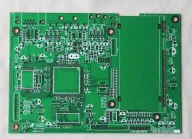
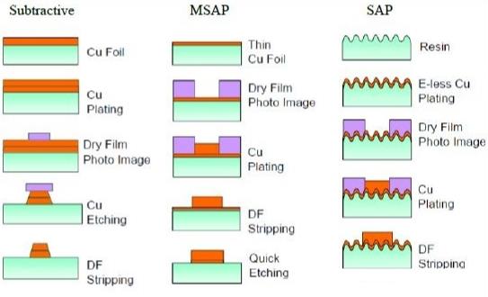
In the process of circuit board layout, after the system layout is completed, the PCB diagram should be reviewed to see whether the system layout is reasonable and whether the optimal effect can be achieved. It can usually be investigated from the following aspects:
1. Whether the system layout guarantees reasonable or optimal wiring, whether the wiring can be carried out reliably, and whether the reliability of the circuit operation can be guaranteed. In the layout, it is necessary to have an overall understanding and planning of the direction of the signal, as well as the power supply and ground wire network.
2. Whether the size of the printed board is consistent with the size of the processing drawing, whether it can meet the requirements of the PCB manufacturing process, and whether there is a behavior mark. This point requires special attention. The circuit layout and wiring of many PCB boards are designed very beautifully and reasonably, but the precise positioning of the positioning connectors is neglected, resulting in the design of the circuit cannot be docked with other circuits.

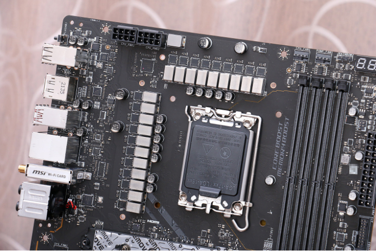
3. Whether the components conflict in two-dimensional and three-dimensional space. Pay attention to the actual size of the device, especially the height of the device. When welding components without layout, the height should generally not exceed 3mm.
4. Whether the layout of the components is dense and orderly, neatly arranged, and whether they are all laid out. In the layout of components, not only the direction of the signal, the type of signal, and the places that need attention or protection must be considered, but the overall density of the device layout must also be considered to achieve uniform density.
5. Whether the components that need to be replaced frequently can be easily replaced, and whether the plug-in board can be easily inserted into the equipment. The convenience and reliability of replacement and connection of frequently replaced components should be ensured.
6. Whether it is convenient to adjust the adjustable components.
7. Whether there is a proper distance between the thermal element and the heating element.
8. Whether there is a radiator or fan installed in the place where heat dissipation is needed, and whether the air flow is unobstructed. Attention should be paid to the heat dissipation of components and circuit boards.
9. Whether the signal direction is smooth and the interconnection is the shortest.
10. Whether the plug, socket, etc. contradict the mechanical design.
11. Is there any consideration for line interference?
12. Whether the mechanical strength and performance of the circuit board have been considered.
13. The artistry and aesthetics of the circuit board layout.
Reasonable division of functional areas
When performing the reverse design of the schematic diagram of a good PCB circuit board, a reasonable division of functional areas can help engineers reduce some unnecessary troubles and improve the efficiency of drawing. Generally speaking, components with the same function on a PCB board are arranged in a concentrated manner, and the division of areas by function can have a convenient and accurate basis when inverting the schematic diagram.
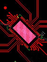
However, the division of this functional area is not arbitrary. It requires engineers to have a certain understanding of electronic circuit related knowledge. First, find the core component in a certain functional unit, and then according to the wiring connection, you can find other components of the same functional unit along the way to form a functional partition. The formation of functional partitions is the basis of schematic drawing. In addition, in this process, don't forget to use the serial numbers of the components on the circuit board cleverly, they can help you partition the functions faster.
Circuit board copy board reverse push principle
1. Correctly distinguish lines and draw wiring reasonably
For the distinction between ground wires, power wires, and signal wires, engineers also need to have relevant power supply knowledge, circuit connection knowledge, PCB wiring knowledge, and so on. The distinction of these lines can be analyzed in terms of the connection of components, the width of the copper foil of the circuit, and the characteristics of the electronic product itself.
In the wiring drawing, in order to avoid the crossing and interpenetration of lines, a large number of grounding symbols can be used for the grounding line. Various lines can use different colors and different lines to ensure that they are clear and identifiable. For various components, special signs can be used, or even Draw the unit circuits separately, and finally combine them.
2. Check and optimize
After the schematic drawing is completed, the reverse design of the PCB schematic can be said to be completed after testing and verification. The nominal value of the components sensitive to the PCB distribution parameters needs to be checked and optimized. According to the PCB file diagram, the schematic diagram is compared and analyzed to ensure that the schematic diagram is completely consistent with the file diagram.