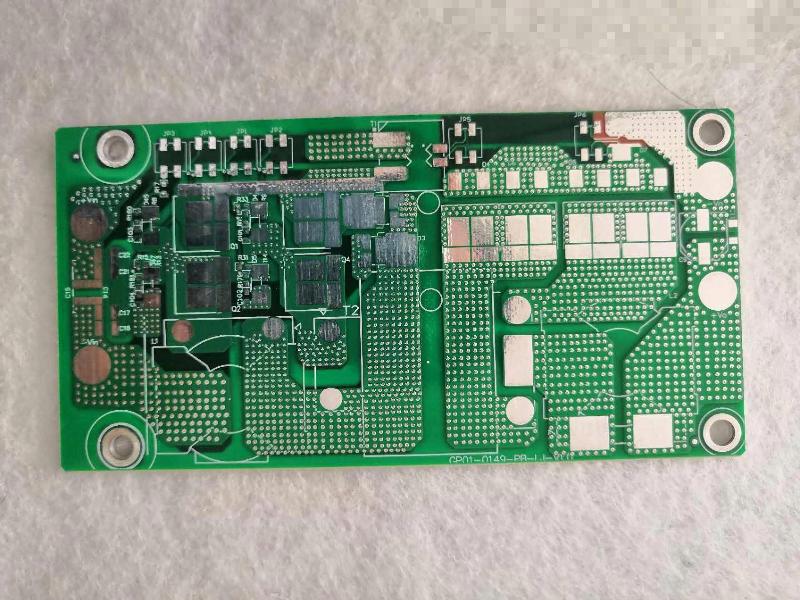
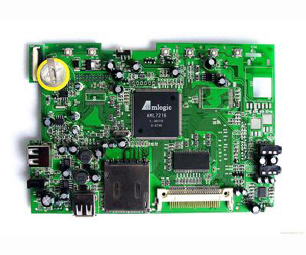
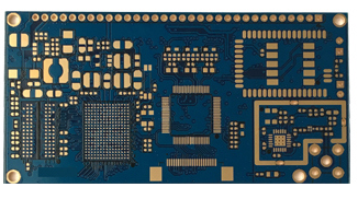
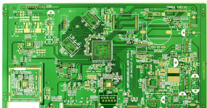
In PCB design, wiring is an important step to complete product design, so it can be said that the preparatory work in front is done for it. In the whole PCB, the design process of wiring is highly limited, with fine skills and large workload. PCB wiring includes single-side wiring, double-side wiring and multi-layer wiring. The means of wiring also has two kinds: automatic wiring and interactive wiring, before automatic wiring, interactive can be used in advance to more strict line wiring requirements, input end and output end edge line should avoid adjacent parallel, lest produce reflex interference. When necessary, ground wire should be added to isolate, and the wiring of two adjacent layers should be perpendicular to each other, which is easy to produce parasitic coupling in parallel.
The distribution rate of automatic wiring depends on good layout, wiring rules can be set in advance, including the number of bending lines, the number of through holes, the number of steps, etc. Undertake exploration type wiring first commonly, connect short line quickly, undertake labyrinth type wiring next, the wiring path that wants cloth to undertake global optimization first, it can disconnect the line that already cloth according to need. And try rewiring to improve the overall effect. For high density PCB design has been felt through hole is not too to adapt, it wasted a lot of valuable wiring channel, in order to solve this contradiction, the blind and buried hole technology, it not only completed the guide hole, also save a lot of wiring channel make wiring process more convenient, more smooth, more perfect, PCB board design process is a complex and simple process, in order to master it well, it needs the majority of electronic engineering designers to experience, to get the true meaning of it.

1. Handling power supplies and ground cables
Even if the wiring in the whole PCB board is completed well, but the interference caused by the power supply and ground wire is not considered well, the performance of the product will decline, and sometimes even affect the success rate of the product. So the wiring of electricity, ground wire should be treated seriously, the noise interference that electricity, ground wire place produces falls to low limit, in order to ensure the quality of the product. For every engineer who is engaged in the design of electronic products, it is clear that the reason for the noise between ground wire and power line is generated.
(1) It is well known that the decoupling capacitor is added between the power supply and ground wire.
(2) As far as possible to widen the width of power supply, ground wire is better than the power line wide, their relationship is: ground wire > power line > signal line, usually signal line width: 0.2 ~ 0.3mm, fine width up to 0.05 ~ 0.07mm, power line 1.2 ~ 2.5mm. The PCB of a digital circuit can be used as a circuit with wide ground conductors, that is, to form a ground network for use (analog ground cannot be used this way)
(3) With a large area of copper layer as ground wire, in the printed board is not used in the place are connected with the ground wire. Or make it multi-layer board, power supply, grounding line each occupy a layer.
2. Common ground processing of digital and analog circuits
Many PCBS are no longer single-function circuits (digital or analog), but are a mix of digital and analog circuits. Therefore, when wiring, we need to consider the interference between them, especially the noise interference on the ground line.
The digital circuit has high frequency and the analog circuit has strong sensitivity. For the signal line, the high frequency signal line should be as far away from the sensitive analog circuit device as possible. For the ground line, the integral PCB has only one node to the outside world, so the problem of digital and analog common ground must be dealt with inside the PCB. In the board, the digital ground and the analog ground are actually separated. They are not connected to each other, but only at the interface (such as plug, etc.) between the PCB and the outside world. There is a bit of a short connection between the digital ground and the analog ground. Note that there is only one connection point. There are also incongruent ones on the PCB, depending on the system design.
3. The signal cable is laid on the electric (ground) layer
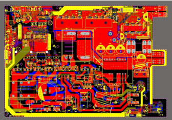
In the multi-layer PCB wiring, because there is no finished line left in the signal line layer, and then add layers will cause waste will also increase the production of a certain amount of work, the cost also increased accordingly, in order to solve this contradiction, you can consider wiring in the electrical (ground) layer. The power zone should be considered first, and the formation second. Because it's good to keep the formation intact.
4. Processing of connecting leg in large area conductor
In the large area of grounding (electricity), the legs of common components are connected with it. The processing of the connecting legs needs to be considered comprehensively. In terms of electrical performance, the pads of component legs are fully connected with the copper surface, but there are some hidden dangers for the welding assembly of components, such as: (1) the welding needs a high power heater. (2) Easy to cause virtual solder joints. Therefore, taking into account the electrical performance and process needs, make a cross welding pad, called heat shield, commonly known as Thermal, so that the possibility of virtual welding spot due to excessive heat dissipation of the section during welding can be greatly reduced. The electrical (ground) leg of the multilayer is treated the same.
5. The role of network system in cabling
In many CAD systems, wiring is determined by the network system. The grid is too dense, the path is increased, but the step is too small, the data volume of the graph field is too large, which will inevitably have higher requirements for the storage space of the equipment, but also has a great impact on the computing speed of computer electronic products. Some paths are invalid, such as those occupied by the pads of component legs or by mounting holes, positioning holes, etc. Too sparse grid and too few paths have a great influence on the distribution rate. Therefore, it is necessary to have a reasonably dense grid system to support the wiring. The legs of standard components are 0.1 inch (2.54mm) apart, so the base of grid systems is usually 0.1 inch (2.54mm) or integral multiples of less than 0.1 inch (e.g. 0.05 inch, 0.025 inch, 0.02 inch, etc.).
6. Checking Design Rules (DRC)
After the wiring design is completed, it is necessary to carefully check whether the wiring design conforms to the rules formulated by the designer, and also to confirm whether the rules formulated meet the requirements of the printed board production process. General check has the following aspects:
(1) Whether the distance between line and line, line and component pad, line and through-hole, component pad and through-hole, through-hole and through-hole is reasonable, whether to meet the production requirements.
(2) Is the width of power cord and ground cable appropriate, and is the coupling between power supply and ground cable tight (low wave impedance)? Is there a place in the PCB where the ground wire can be widened?
(3) Whether good measures are taken for the key signal lines, such as short length, protective lines, input lines and output lines are clearly separated.
(4) Whether the analog circuit and the digital circuit have their own independent ground wires.
(5) Whether the graphics (such as ICONS and notations) added to PCB will cause signal short circuit.
(6) Modify some unsatisfactory lines.
(7) Is there any process line on PCB? Whether the resistance welding meets the requirements of the production process, whether the resistance welding size is appropriate, whether the character mark is pressed on the welding pad of the device, so as not to affect the quality of electric equipment.
(8) Whether the outer frame edge of the power supply layer in the multi-layer board is reduced, such as the copper foil exposed outside the board of the power supply layer is easy to cause short circuit.